Download
1 / 8
80 likes | 222 Views
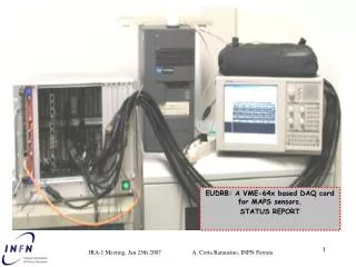
EUDRB: A VME-64x based DAQ card for MAPS sensors. STATUS REPORT. A VME-64x based DAQ card for MAPS sensors. EUDRB card: status report. Reported here: A “MIMO*2” version of the EUDRB (A. Cotta Ramusino) featuring: JTAG configuration of the MIMO*2

E N D
EUDRB: A VME-64x based DAQ card for MAPS sensors. STATUS REPORT JRA-1 Meeting, Jan 25th 2007 A. Cotta Ramusino, INFN Ferrara
A VME-64x based DAQ card for MAPS sensors EUDRB card: status report • Reported here: • A “MIMO*2” version of the EUDRB (A. Cotta Ramusino) featuring: • JTAG configuration of the MIMO*2 • FPGA design specific for MIMO*2 timing and data structure • Optimized VME interface with improved MBLT bandwidth • Larger set of diagnostic routines running on the NIOS-II on-board processor to implement the “Development” operating mode on the unit delivered today to the University of Geneva’s DPNC • A “MIMOSA V” version of the EUDRB (D. Spazian) featuring: • USB 2.0 interface • FPGA design specific for MIMOSA V timing and data structure • LabView based test setup JRA-1 Meeting, Jan 25th 2007 A. Cotta Ramusino, INFN Ferrara
A VME-64x based DAQ card for MAPS sensors MIMO*2 - EUDRB card: works in progress • Features of the “MIMO*2” - EUDRB delivered to Univ. Geneve - DPNC: • JTAG configuration of the MIMO*2 : the ‘C++’ library designedbyGilles Claus of IRES-LEPSI, Strasbourg has been turned into a set of ‘C’ routines executed by the NIOS-II to configure the MIMO*2 chip via the dedicated RJ45 connector on the EUDRB-DCD • FPGA design specific for MIMO*2 timing and data structure : this FPGA design takes into account the dummy pixels and the MIMO*2 reset timing. In the current “development” stage, the FPGA acquires data in Non Zero Suppressed mode when receiving a “software” trigger but produces a “Zero Suppressed mode” output packet to exploit the on-board output FIFO and the MBLT-mode operation of the VME interface. • Optimized VME interface with improved MBLT bandwidth : a set of new entries for the MIMO*2 configuration and the “software” trigger generation has been added to the board’s VME address space. The board response time to the MBLT accesses has been improved: • a single transfer in an MBLT block now completes in ~190ns (~42MB/s peak BW) of which about 90ns are due to the EUDRB and 100ns to the MVME6100 CPU • Larger set of diagnostic routines running on the NIOS-II on-board processor: the board can be operated from VME or even from the NIOS II UART. In the present “development” stage the NIOS-II acknowledges VME commands and writes diagnostic messages to its UART output port to help in the system-level debugging JRA-1 Meeting, Jan 25th 2007 A. Cotta Ramusino, INFN Ferrara
A VME-64x based DAQ card for MAPS sensors MIMO*2 - EUDRB card: Optimized VME interface with improved MBLT bandwidth c a b d L.Chiarelli, A.Cotta R., Jan 19 2007 • Detail of the MBLT block read. • The cycle time between two successive transfers is 187ns (-> 42 MB/s peak transfer rate, compared to the maximum theoretical rate of 80MB/s claimed by the standard). This time is made up of • (a) Delay from nDS0,nDS1 active to nDTACK active: about 60ns. It is determined by the EUDRB. • (b) Delay from nDTACK active to nDS0,nDS1 unactive : about 50ns. It is determined by the VME CPU • (c) Delay from nDS0,nDS1 unactive to nDTACK unactive : about 30ns. It is determined by the EUDRB. • (d) Delay from nDTACK active to nDS0,nDS1 unactive : about 50ns. It is determined by the VME CPU JRA-1 Meeting, Jan 25th 2007 A. Cotta Ramusino, INFN Ferrara
A VME-64x based DAQ card for MAPS sensors MIMO*2 - EUDRB card: diagnostic routines running on the NIOS-II on-board processor Room Lights were ON!!! JRA-1 Meeting, Jan 25th 2007 A. Cotta Ramusino, INFN Ferrara
A VME-64x based DAQ card for MAPS sensors MIMO*2 - EUDRB card: example sequence of commands written via VME EXAMPLE VME COMMANDS: 1) preparing for the trigger sh-2.05a# ./test -w0x30000000 -a1 -d0x20 -n1 address = 30000000 addressspace = 1 sh-2.05a# 2) trigger !!! sh-2.05a# ./test -w0x30000010 -a1 -d0xa0000000 -n1 address = 30000010 addressspace = 1 sh-2.05a# 3) Check OUTFIFO Not Empty (bit 1 of the EUDRB Ctrl/Status register) sh-2.05a# ./test -r0x30000000 -a1 -n1 address = 30000000 addressspace = 1 DATA=27 sh-2.05a# 4) Readout in MBLT mode !!! sh-2.05a# ./test -r0x30400000 -a3 -m131120 > pippo2301_16.31.txt sh-2.05a# 5) cleanup !!! sh-2.05a# ./test -w0x30000010 -a1 -d0xc0000000 -n1 address = 30000010 addressspace = 1 HEADER TRAILER “test” is a function based on the library written by L. Chiarelli (Univ. Ferrara) for the MVME6100 !!! MESSAGES APPEARING AT THE NIOS-II SERIAL OUTPUT!!!: EdgeCap_USBVME_CTRL_IN = 16385 Serving USBVME_CMD. Command received: c0000000 VME CMD Returning from ClearTrigProcUnits JRA-1 Meeting, Jan 25th 2007 A. Cotta Ramusino, INFN Ferrara
A VME-64x based DAQ card for MAPS sensors MIMOSA V - EUDRB card: works in progress • The debugging of the MIMOSA V FPGA design goes on: • USB 2.0 interface : reliable link established from PC (LabView) to FPGA for passing the MIMOSA V configuration parameters, timing unit configuration parameters and “software” triggers • FPGA design specific for MIMOSA V timing and data structure • the timing unit controlling the acquisition of the AD samples into the SRAMs is operating reliably at up to 20MHz: the operation of this internal logic blocks in Non Zero Suppressed mode has been fully debugged, thanks to the use of the “Signal Tap” tool from ALTERA which allows the “spying” of the internal activity of the FPGA. • Some corruption of the data received by the PC on the USB link still present. More investigation is needed on the system to exclude an hardware problem with the USB • Full simulation of the FPGA design for the operation in Zero Suppressed mode has been completed and it is soon to start the debugging with the “Signal Tap” tool JRA-1 Meeting, Jan 25th 2007 A. Cotta Ramusino, INFN Ferrara
A VME-64x based DAQ card for MAPS sensors EUDRB card: status report • Next Milestones: • MIMO*2-EUDRB (A. Cotta R.): • confirm that what appeared to be an hardware problem with the upper memory banks was really a firmware bug ( all memory seems to work after the MIMO*2 specific FPGA design has been implemented) -> start the production of new boards • implement and test the module written by D. Spazian to interface the TLU • implement and test the logic for the Zero Suppressed operation mode of the MIMO*2 specific FPGA design • characterize the analog performances of the board ( with help from M. Jastrzab, Univ. Crakow/Univ. Como) • implement and test the USB2.0 interface with the specific changes needed to account for the parameters needed to configure the MIMO*2 • MIMOSA V-EUDRB (D.Spazian): • implement and test the module to interface the TLU • implement and test the logic for the Zero Suppressed operation mode of the MIMOSA V specific FPGA design • tune the analog performances of the board for the MIMOSA signal level ( with help from M. Jastrzab) • implement and test the VME interface • System tasks (Lorenzo Chiarelli): • writing a library of functions to configure monitor and readout the EUDRBs JRA-1 Meeting, Jan 25th 2007 A. Cotta Ramusino, INFN Ferrara