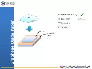
Download
1 / 11
690 likes | 1.68k Views
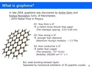
What is graphene?. In late 2004, graphene was discovered by Andre Geim and Kostya Novoselov (Univ. of Manchester). - 2010 Nobel Prize in Physics . Q1. How thick is it? a million times thinner than paper ( The interlayer spacing : 0.33~0.36 nm) Q2. How strong is it?

E N D
What is graphene? In late 2004, graphene was discovered by Andre Geim and KostyaNovoselov (Univ. of Manchester). - 2010 Nobel Prize in Physics • Q1. How thick is it? • a million times thinner than paper • (The interlayer spacing : 0.33~0.36 nm) • Q2. How strong is it? • stronger than diamond • (Maximum Young's modulus : ~1.3 TPa) • Q3. How conductive is it? • better than copper • (The resistivity : 10−6Ω·cm) • (Mobility: 200,000 cm2 V-1 s-1) But, weak bonding between layers Seperated by mechanical exfoliation of 3D graphite crystals.
Molecular structure of graphene 2D graphene sheet Carbon Electrons move freely across the plane through delocalized pi-orbitals CNT bucky ball 3D graphite
Electronic structure of graphene Effective mass (related with 2nd derivative of E(k) ) Massless Graphene charged particle is massless Dirac fermion. Zero gap semiconductor orSemi-metal Pz anti bonding Conduction band Ef K Fermi energy K’ Pz bonding Valence band K 2DEG K’
Electrical properties of graphene High electron mobilityat room temperature: Electronic device. Si Transistor, HEMT devices are using 2D electron or hole. μ (mobility) = vavg/ E(velocity/electric field) Jdrift ~ ρx vavg
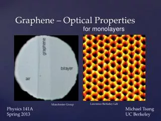
Optical properties of graphene Optical transmittance control: transparent electrode Reduction of single layer: 2.3% F. Bonaccorso et al. Nat. Photon.4, 611 (2010)
Mechanical properties of graphene Mechanical strength for flexible and stretchable devices Young’s modulus =tensile stress/tensile strain Diamond ~ 1200 GPa Force-displacement measurement C. Lee et al. Science321, 385 (2008)
Graphene growth by chemical vapor deposition SiC sublimation Metal catalysis CVD Ni: non uniform multi Cu: uniform single Cu: layer by layer growth Current Status Solid Carbon : Low temp. Nat.mat.2009.203. Ar1atm,1450~1650°C Terrace size increase. Nat.2010.549. ACS nano,2011 High temperature growth :1200~1500°C Non-uniform growth in Step edge and terrace. High cost SiC wafer : SiC growth on Si No transfer required Low temperature growth :below 1000°C Unform growth : Capet like (Large area) Si CMOS compatible process. “Transfer required” Pros& Cons
Large area graphene K. S. Kim et al. Nature457, 706 (2009) S. Bae et al. Nat. Nano.5, 574 (2010)
PSCs with graphene anodes a b PEDOT :PSS PTB7 -F40 TiOx Al 3.3 4.3 4.3 4.3 5.0 5.1 5.4 6.0 GR/PEDOT: PSS (DT) PC71BM 8.0 eV
PLEDs with graphene anodes Al Ca PEDOT :PSS SY 2.4 2.9 4.3 4.8 eV 5.1 GR/PEDOT: PSS (DT) 5.4