Surface micromachining and Process flow part 1
570 likes | 1.09k Views
Surface micromachining and Process flow part 1. Identify the basic steps of a generic surface micromachining process Identify the critical requirements needed to create a MEMS using surface micromachining

Surface micromachining and Process flow part 1
E N D
Presentation Transcript
Surface micromachining and Process flow part 1 • Identify the basic steps of a generic surface micromachining process • Identify the critical requirements needed to create a MEMS using surface micromachining • List common structural material/sacrificial material/etchant combinations used in surface micromachining • Compare and contrast the relative merits of wet micromachining versus dry micromachining • Explain the phenomenon of stiction, why it occurs, and methods for avoiding it • Describe the process of lift-off • Explain what is meant by packaging and describe the ways in which it present major challenges in MEMS • Define the terms • Structural layer/material • Sacrificial layer/material, • Release, and • Die separation • Develop a basic-level process flow for creating a simple MEMS device
Surface micromachining SomeJengapieces are removed. The onesthatremainformthe MEMS structure. The Si waferfunctionslikethebiggreen flat plate. + = Surface micromachining
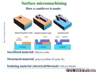
Review of surface micromachining process Surface micromachining example – Creating a cantilever Deposit poly-Si (structural layer—the Jenga pieces that remain) Deposit SiO2(sacrificial layer—the Jenga pieces that are removed) Remove sacrificial layer (release) Etchpart of thelayer. Often the most critical Silicon wafer (Green Lego® plate)
Reminder of the surface micromachining process top view side view silicon oxide metal
Process flow for surface μ-machined cantilever Mask 1 (positive resist) Mask 1 (negative resist) . . . . . . Top view (4) Top view (5) Top view (6)
Process flow for surface μ-machined cantilever . . . . . . Mask 2 (positive resist) Mask 2 (negative resist) Top view (7) Top view (9) Top view (11) Top view (10)
History and processes • Surface micro-machining (SMM) • Developed in the early 1980s at the University of California at Berkeley • Originally for polysiliconmechanical structures • Other processes include • Sandia National Lab’s SUMMIT (Sandia’s Ultra-planar Multi-level MEMS Technology) five levels possible with four poly layers • MEMS CAP’s polyMUMPs (Multi User MEMS Processes) three layers of poly with a layer of metal Photo of a PolyMUMPs surface-micromachinedmicro-mirror. The hinge design allows for out-of-plane motion of the mirror.
Requirements and advantages • Three to four different materials required in addition to the substrate • Sacrificial material (etch rate Rs) • Structural mechanical material (etch rate Rm) • Sometimes electrical isolators and/or insulation materials (etch rate Ri) • Many SMM processes are compatible with CMOS (complementary metal oxide silicon) technology used in microelectronics fabrication. • Can more easily integrate with their control electronics on the same chip • Many SMM processes have developed their own sets of standards Rs>> Rm> Ri Best results are obtained when structural materials are deposited with good step coverage. Chemical vapor deposition (CVD) or Physical vapor deposition (PVD) If PVD Sputtering or Evaporation efficient and inexpensive
Common material/etchant combinations for surface μ-machining
Problems and issues • Wet etching • 40 years of experience and data in the semiconductor industry • Ability to remove surface contaminants • Very high selectivities • Usually isotropic always involve undercutting • Dry etching • Better resolution than wet etching • More directionality (High aspect ratios ) • Lower selectivities • No undercutting Stiction moisture
Stiction • Stiction = static + friction • Stiction = stick + friction An example of a portmanteau • Ways to reduce stiction • Coat (cubrir) surface with a thin hydrophobiclayer in order to repel liquid • Dry surfaces using supercritical CO2. Removes fluids without allowing surface tension to form. • Use “stand-off bumps” on the underside of moving parts. Pillars prop up (soportar) movable parts An example of an unfavorable scaling C
Problems and issues “Dimple” resulting from a stand-off bump on the underside of the cold arm • Polysiliconhotarm actuator created using surface μ-machining
Tetoca a ti • Explain (with words, drawings, or both) how standoff bumps might be created.
Lift-off • Usually included as an “additive technique” by most authors • Photoresist is spun on a wafer and exposed to create pattern • Resist has either straight side walls, or better, a reentrant shape. • Material deposited through the photoresist mask using a line-of-sight method, such as evaporation • Shadowing takes place, • Part of the photoresist sidewalls must be free of deposited material • Photoresist stripped leaving behind only material deposited through the opening. Unwanted material is lifted off. (+) or (-) resist? C Thickness of the deposited material must be thin compared to the resist thickness. Most often used to deposit metals, especially those that are hard to etch using plasmas
Typical process steps for surface micromachining • modeling and simulation • design a layout • design a mask set C thin film formation (by growth or deposition) 1 2 3 4 mask set • This is where process flow becomes complicated. lithography etching C die separation release packaging
Die separation and packaging • Must separate the individual devices • Often saw or scribe the wafer • Provide MEMS device with electrical connections • Protect MEMS from the environment • Sometimes must also provide limited access to environment (e.g., pressure sensor, inkjet print heads) • Packaging a difficult engineering problem • Largest cost of producing many (most) devices C die separation packaging packaging
More on packaging • Wafer-level packaging • Die-level packaging packaging
More on packaging • Schematic of a packaged MEMS pressure detector showing some of the requirements unique to MEMS
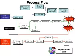
Process integration (Process flow) • How do we put these things together to create a device? • Specifically: • How do we choose which steps we need? • How do we choose the orderof the steps? • How do we communicate this order of steps in the field? • We have learned much about the many materials and techniques for used processing materials to create devices, including • Nature of crystalline silicon • Adding material • Doping • Oxidation • Deposition • PVD • CVD • Photolithography • Bulk Micromachining • Surface Micromachining Process integration (Process flow) List of process steps in the correct order with the accompanying lithography masks.
Process integration (Process flow) “Process flow” está acá. Hemospasado mucho tiempo acá. http://juliaec.files.wordpress.com/2011/04/blooms_taxonomy.jpg http://ictintegration.wikispaces.com/Bloom
Bulk μ-machined pressure sensor Thin Si diaphragm changes shape when pressure changes on one side relative to the other. Piezoresistors (implemented using p+ diffusion) sense the deformation. Aluminum wires send resistive electrical signal off the chip. n+diffusion is used as an etch stop for the backside etch. Oxide + Nitride provides wafer protection for backside etch and insulator between Al wires and wafer.
Process flow, pass 1 The first pass for determining the process flow is to decide which steps we need. • What are the basic steps necessary to build the diaphragm? • Etch backside • (Need to protect front of wafer during backside etch) • Add SiO2 and nitride layers • Etch area above diaphragm to give diaphragm ability to move easily • Create an “etch stop” layer • Reverse bias p-n junction will stop etch • Start with p-type wafer • Dope n-type layer or grow n-type epilayer (layer produces with epitaxy)
Process flow, pass 1 The first pass for determining the process flow is to decide which steps we need. • What are the basic steps necessary to build the sensor? • Add diffusion to get piezoresistor • Add wires so that piezoresistor can be connected to external world • Note that wires must be metal (Could use diffusion if the distance is short)
Process flow, pass 1 The first pass for determining the process flow is to decide which steps we need. • What processing steps are required to produce entire device? • Deposit/pattern oxide and nitride • Deposit/pattern Al for pads • Backside etch • n-type diffusion for etch stop • p-type diffusion for resistors/wires Each of these steps results in more steps in the detailed process flow. But to begin, let’s determine the order in which the steps must be placed.
Process flow, pass 1 Order of steps • What impacts our decisions on choosing an order? • Geometry • The oxide must be deposited before the nitride. • Temperature • High T processes mustgo first. High T processes can cause dopants to further diffuse and metals to melt and flow. • Which processes are high T? • Oxidation • CVD (unless PECVD) • Drive-in for diffusion • Mechanical stress • If a following step can cause a device to break, you may want to rethink the order if you can. This is why release steps are often (though not always) done last. • Interaction of chemicals • If an etch will attack another material, you must either place is earlier in the process flow or protect the material.
Process flow, pass 1 Order of steps • Let’s choose an order • n-type doping • Oxide: Can be done before doping of resistors if oxide is thin. (Boron will implant through thin oxide but not if oxide is thick!) • Dope resistors • Deposit nitride Mask 1 Do we do backside etch or metallization next? A long backside etch will attack metal, and so we must do backside etch first. Can we pattern nitride and oxide on both front and back at the same time? Yes, but etching both sides at the same time will etch all the way through the silicon and you will not have a diaphragm! And so we do them at different times because need to protect the front side during backside etch.
Process flow, pass 1 Order of steps Let’s choose an order Backside etch: Before etching backside, we must cut the nitride and SiO2 using Mask 2. Nitride and SiO2 on topside protects topside of wafer. Front side etch: Etch nitride and oxide on topside of wafer Metallization: How does the metal connect to the doping? Must cut through the nitride and oxide first. Holes are called “vias” or “contact cuts”. Must pattern oxide and nitride on topside of wafer to create contact cuts.. Metallization: Add aluminum for vias and pads Podemoscombinarlos, ¿no? 6 Mask 3 7 Mask 2
Pass 2, Detailed process flow • A detailed process flow is the list of all steps necessary for the process people to implement the device. It should include each of the following: • All steps in the proper order, including when to clean the wafer • Any chemicals necessary • Thicknesses of materials • These choices come for modeling. • The “process people” can turn chemicals and thicknesses into times necessary for etches, depositions, etc. • Equipment necessary • It is the responsibility of the process flow person to think about which equipment is necessary for each step. Why? Because if you need a high temperature deposition to follow a metallization, you need a PECVD to do it or your metal will flow. The process flow person knows the entire process and makes design decisions. • MASKS for photoligthography
Detailed process flow • Let’s revisit each of the basic steps that we came up with and see what is really involved. You will notice that many of the steps actually turn into several steps when coming up with the detailed process flow. For this exercise, we will ignore dimensions and chemicals. However, note that these are also important components of the design flow. • n-type doping • No mask is required since it covers the entire wafer • This could be done by purchasing a wafer with an epilayer or it requires 2 steps • implantation • drive-in • Oxide • No mask is required since it covers the entire wafer. • Note that oxide will grow on both sides of the wafer. If you do not want it on the backside of the wafer, you must protect the backside of the wafer. • In this case, we do want oxide on both sides of the wafer.
Detailed process flow Mask 1 • Dope resistors and wires • Mask 1 – what does it look like? (Assume positive resist.) • This step requires 4 total steps • Photolithography so that ion implantation only goes where you want it to go • Ion implantation • Remove photoresist (Must be done before drive-in. Why?) • Drive-in • Deposit nitride • No mask is required since it covers the entire wafer • Depending on the process, you may need to process both sides of the wafer. • PVD often only deposits on one side of the wafer. • CVD often deposits on both sides of the wafer Mask 1
Detailed process flow Mask 2 • Backside etch • Mask 2 – what does it look like? (Assume positive resist.) • Must align Mask 2 with Mask 1 so that the resistors are on the edge of the diaphragm. Alignment marks • This step requires 5 steps • Photolithography to determine where you want the backside etch to start • Etch nitride • Etch SiO2 • Etch Si (Nitride and the SiO2used as a “hard mask” for the long Si etch.) • Remove photoresist Mask 2
Detailed process flow Mask 3 • Contact Cuts/Diaphragm cut • Mask 3 – what does it look like? (Assume positive resist.) • Must align Mask 3 with Mask 1 so that wires connect to resistors. Alignment marks • This step requires 3 total steps • Photolithography to determine where you want material removed for the metal • Etch the nitride and oxide • Remove the photoresist Mask 3
Detailed process flow Mask 4 • Metallization • Mask 4 – what does it look like? (Assume positive resist.) • Must align Mask 4 with Mask 1 so that metal does not etch away. Alignment marks • This step requires 4 total steps • Deposit the Aluminum • Photolithography to determine which Al you want to remove • Etch unwanted Al • Remove the photoresist Mask 4
Pass 3, Final process flow • These steps can be combined to create a final process flow. • One additional requirement in process flows is to include information about when to clean the wafer. Some general guidelines are: • Always start with an RCA clean and an HF dip to get rid of every possible • All future cleans are usually RCA cleans without an HF dip. HF may etch away your MEMS structures. • Alwaysstrip photoresist and clean before high temperature processes. • Alwaysclean before depositing a new layer.
Final process flow • Final Process Flow for Bulk Micromachined Pressure Sensor • Starting material: 100mm (100) p-type silicon, 1×1015cm-3 boron Clean: Standard RCA clean with HF dip Oxide: Grow SiO2 on both sides of wafer Photolithography: Mask 1 (alignment) Note: since the first patterned material is diffusion, which you cannot see, you must add alignment marks in the wafer or the first material you can see. If the first patterned material is something you can see, you do not need a separate alignment mark mask. Etch: Etch alignment marks into SiO2. Strip: Strip photoresist Note: since the next step is not a material deposition or a high temp step, a clean is not necessary. Photolithography: Mask 2 (piezoresistors) Implant: Ion implantation of boron to achieve 1×1019cm-3 at surface after drive-in Strip: Strip photoresist Note: following step is a high temp step, so must clean wafer before. Clean: RCA cleans, no HF dip Drive-in: Drive in diffusion to achieve 0.2 μm junction depth Note: following step is a material deposition, so must clean wafer before. Clean: RCA cleans, no HF dip Nitride: Deposit 50 nm silicon nitride using LPCVD Photolithography: Mask 3 (backside photolithography for the diaphragm) Etch: Remove nitride and oxide from back of wafer Backside etch: Etch backside with KOH using electrochemical etch stop Note: photoresist strip not necessary since returning to topside of wafer and strip will be done later for topside processing. Photolithography: Mask 4 (vias/diaphragm opening) Etch: Plasma etch nitride and oxide for vias and diaphragm opening Strip: Strip photoresist Clean: RCA cleans, no HF dip Metal: Deposit 1 μm of aluminum Photolithography: Mask 5 (aluminum) Etch: Remove Al with PAN etch Strip: Strip photoresist Sinter: Anneal contacts at 425°C, 30 minutes C C