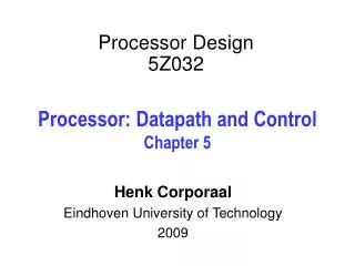
Processor Design
Processor Design. Clocking Methodology Defines when signals can be read and written Going to assume an edge triggered clocking methodology. Control Step. Each control step takes one clock cycle. Source registers output here. Destination registers read values here. Clock cycle.

Processor Design
E N D
Presentation Transcript
Processor Design • Clocking Methodology • Defines when signals can be read and written • Going to assume an edge triggered clocking methodology
Control Step • Each control step takes one clock cycle Source registers output here Destination registers read values here Clock cycle Signals propagate through system
S t a t e C o m b i n a t i o n a l l o g i c e l e m e n t
Datapath Design Chapter 5 P & H
Introduction • Designing an implementation which contains subset of core MIPS instruction set: • Memory reference instructions (lw & sw) • Arithmetic-logic instructions (add, sub, and, or and slt) • Branch and jump instructions (beq, j)
Overview of Implementation • Consider execution of an instruction • First two steps identical • Use PC to fetch an instruction from memory • Read 1 or 2 registers as specified in instruction • Rest of steps dependent on instruction class • Most will use ALU • Many write value back to register file
Overview of Implementation • Will start with simple single cycle implementation • Implementation will comprise datapath plus control
A d d 4 R e a d P C a d d r e s s I n s t r u c t i o n I n s t r u c t i o n m e m o r y Instruction Fetch
R-type Instructions • All R-type instructions: • Read two registers • Perform some ALU operation • add, sub, slt, and, or, etc. • Write the result back to the register file
A L U c o n t r o l 5 R e a d r e g i s t e r 1 R e a d d a t a 1 5 R e g i s t e r R e a d Z e r o r e g i s t e r 2 n u m b e r s R e g i s t e r s D a t a A L U A L U 5 W r i t e r e s u l t r e g i s t e r R e a d d a t a 2 W r i t e D a t a d a t a R e g W r i t e a . R e g i s t e r s b . A L U Components 3
A L U o p e r a t i o n 3 R e a d r e g i s t e r 1 R e a d d a t a 1 R e a d Z e r o r e g i s t e r 2 I n s t r u c t i o n R e g i s t e r s A L U A L U W r i t e r e s u l t r e g i s t e r R e a d d a t a 2 W r i t e d a t a R e g W r i t e Datapath for R-Type Instructions
lw and sw Instructions • lw $7, offset($8) or sw $7, offset($8) • These instructions • Compute the memory address (16 bit signed offset + base register) • If sw then value must also be loaded from reg file • If lw the value read from memory must be stored to reg file • rs contains base, rt contains src/dst register • Need to sign-extend offset to 32-bit value • OP, RS, RT are same format/place as w/ R-type • Simplicity favours regularity
A L U o p e r a t i o n 3 R e a d r e g i s t e r 1 M e m W r i t e R e a d d a t a 1 R e a d Z e r o r e g i s t e r 2 I n s t r u c t i o n A L U R e g i s t e r s A L U R e a d W r i t e r e s u l t A d d r e s s d a t a r e g i s t e r R e a d d a t a 2 W r i t e D a t a d a t a m e m o r y W r i t e R e g W r i t e d a t a 1 6 3 2 S i g n M e m R e a d e x t e n d Datapath for lw and sw
beq Instruction • beq $7, $8, offset • if ($7 == $8) then pc <= pc + 4 + (offset << 2)else pc <= pc + 4
P C + 4 f r o m i n s t r u c t i o n d a t a p a t h A d d S u m B r a n c h t a r g e t S h i f t l e f t 2 A L U o p e r a t i o n 3 R e a d r e g i s t e r 1 I n s t r u c t i o n R e a d d a t a 1 R e a d r e g i s t e r 2 T o b r a n c h R e g i s t e r s A L U Z e r o c o n t r o l l o g i c W r i t e r e g i s t e r R e a d d a t a 2 W r i t e d a t a R e g W r i t e 1 6 3 2 S i g n e x t e n d beq datapath
Simple Implementation Scheme • All instructions execute in single clock cycle: • No data path resource used more than once per clock cycle • Components of different instruction classes may be shared if no conflicts occur • May require multiple connections to same input • Multiplexer used to select appropriate input
Combining datapath for R-type and memory instructions • Datapaths very similar • Two main differences • Second input to ALU is a register (for R-type) or sign-extended lower half of instruction (lw and sw) • Value stored in dest register comes from ALU (R-type) or memory (lw)
A L U o p e r a t i o n 3 R e a d r e g i s t e r 1 R e a d d a t a 1 R e a d Z e r o r e g i s t e r 2 I n s t r u c t i o n R e g i s t e r s A L U A L U W r i t e r e s u l t r e g i s t e r R e a d d a t a 2 W r i t e d a t a R e g W r i t e Datapath for R-Type Instructions
A L U o p e r a t i o n 3 R e a d r e g i s t e r 1 M e m W r i t e R e a d d a t a 1 R e a d Z e r o r e g i s t e r 2 I n s t r u c t i o n A L U R e g i s t e r s A L U R e a d W r i t e r e s u l t A d d r e s s d a t a r e g i s t e r R e a d d a t a 2 W r i t e D a t a d a t a m e m o r y W r i t e R e g W r i t e d a t a 1 6 3 2 S i g n M e m R e a d e x t e n d Datapath for lw and sw
R e a d r e g i s t e r 1 R e a d d a t a 1 R e a d r e g i s t e r 2 I n s t r u c t i o n R e g i s t e r s R e a d R e a d W r i t e d a t a 2 d a t a r e g i s t e r M M u u W r i t e x D a t a x d a t a m e m o r y W r i t e d a t a 1 6 3 2 S i g n e A L U o p e r a t i o n 3 M e m W r i t e M e m t o R e g A L U S r c Z e r o A L U A L U A d d r e s s r e s u l t R e g W r i t e M e m R e a d x t e n d Combined Datapath
A d d 4 R e g i s t e r s R e a d A L U o p e r a t i o n 3 M e m W r i t e r e g i s t e r 1 R e a d P C R e a d M e m t o R e g R e a d a d d r e s s d a t a 1 r e g i s t e r 2 A L U S r c Z e r o I n s t r u c t i o n A L U R e a d A L U R e a d W r i t e A d d r e s s r e s u l t d a t a 2 r e g i s t e r d a t a M M u I n s t r u c t i o n u W r i t e x D a t a x m e m o r y d a t a m e m o r y W r i t e R e g W r i t e d a t a 1 6 3 2 S i g n M e m R e a d e x t e n d Adding Datapath for instruction fetch
P C S r c M A d d u x A L U A d d 4 r e s u l t S h i f t l e f t 2 R e g i s t e r s A L U o p e r a t i o n 3 R e a d M e m W r i t e A L U S r c R e a d r e g i s t e r 1 P C R e a d a d d r e s s R e a d M e m t o R e g d a t a 1 Z e r o r e g i s t e r 2 I n s t r u c t i o n A L U A L U R e a d W r i t e R e a d A d d r e s s r e s u l t M d a t a r e g i s t e r d a t a 2 M u I n s t r u c t i o n u x W r i t e m e m o r y D a t a x d a t a m e m o r y W r i t e R e g W r i t e d a t a 3 2 1 6 S i g n M e m R e a d e x t e n d Add in beq components
For R-Type instructions need to perform operation dependent of function field For load instructions use ALU to compute memory address by addition For branch instructions ALU used for subtraction ALU Control
Truth Table for ALU control • Note multiple levels of control • Main control unit generates ALUOp • ALU control generates operation
Main Control Unit Design • Opcode fields always bits 31 – 26 (Op[5-0]) • Two regs to be read are always rs and rt • Base reg for loads and stores always rs • 16 bit offset always bits 15 – 0 • Destination register is in one of two places • r-type instructions RD • lw it is RT
P C S r c 1 M A d d u x A L U 0 4 A d d r e s u l t S h i f t R e g W r i t e l e f t 2 I n s t r u c t i o n [ 2 5 – 2 1 ] R e a d r e g i s t e r 1 R e a d M e m W r i t e R e a d P C d a t a 1 I n s t r u c t i o n [ 2 0 – 1 6 ] a d d r e s s R e a d M e m t o R e g A L U S r c r e g i s t e r 2 Z e r o I n s t r u c t i o n R e a d 1 A L U A L U [ 3 1 – 0 ] 1 R e a d W r i t e d a t a 2 1 A d d r e s s r e s u l t M r e g i s t e r M d a t a u M I n s t r u c t i o n u I n s t r u c t i o n [ 1 5 – 1 1 ] x W r i t e u x m e m o r y R e g i s t e r s x 0 d a t a 0 D a t a 0 W r i t e m e m o r y R e g D s t d a t a 1 6 3 2 S i g n I n s t r u c t i o n [ 1 5 – 0 ] e x t e n d A L U M e m R e a d c o n t r o l I n s t r u c t i o n [ 5 – 0 ] A L U O p Datapath
0 M u x A L U A d d 1 r e s u l t A d d S h i f t P C S r c l e f t 2 R e g D s t 4 B r a n c h M e m R e a d M e m t o R e g I n s t r u c t i o n [ 3 1 2 6 ] C o n t r o l A L U O p M e m W r i t e A L U S r c R e g W r i t e I n s t r u c t i o n [ 2 5 2 1 ] R e a d R e a d r e g i s t e r 1 P C R e a d a d d r e s s d a t a 1 I n s t r u c t i o n [ 2 0 1 6 ] R e a d Z e r o r e g i s t e r 2 I n s t r u c t i o n 0 R e g i s t e r s A L U R e a d A L U [ 3 1 – 0 ] 0 R e a d W r i t e A d d r e s s M d a t a 2 r e s u l t 1 d a t a I n s t r u c t i o n r e g i s t e r M u M u m e m o r y x u I n s t r u c t i o n [ 1 5 1 1 ] W r i t e x D a t a 1 x d a t a 1 m e m o r y 0 W r i t e d a t a 1 6 3 2 I n s t r u c t i o n [ 1 5 0 ] S i g n e x t e n d A L U c o n t r o l I n s t r u c t i o n [ 5 0 ] Datapath with Control Unit