Download
1 / 41
420 likes | 642 Views
Van de Graaff Accelerators Utilizations in Materials Research. Sufian Abedrabbo. TMS Educational Resource Awards. OUTLINE. Abstract Introduction Ion Beam Mixing in Materials Research Experimental Setup – Ion-Beam Mixing, Rutherford Backscattering Conclusions Acknowledgment.

E N D
Van de Graaff Accelerators Utilizations in Materials Research Sufian Abedrabbo TMS Educational Resource Awards
OUTLINE • Abstract • Introduction • Ion Beam Mixing in Materials Research • Experimental Setup – Ion-Beam Mixing, Rutherford Backscattering • Conclusions • Acknowledgment
ABSTRACT • An overview of processes enabled by the Availability of Accelerators (Van de Graaff) / Ion Implanters. • In particular Results of: - Ion Beam Assisted Surface Modification (IM) of Semiconductors, - Silicon-on-Insulators Formation are Briefed. - Structural Analysis Capabilities - Rutherford Backscattering (RBS).
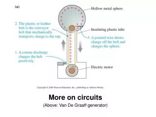
INTRODUCTION • Van de Graaff accelerator is one of many types of accelerators available today. • In a University, Accelerators / Implanters provide tremendous capabilities: a) Ion Beam Assisted Surface Modification (IM) is a very powerful technique by which non-equilibrium or meta-stable alloys and inter- metallic compounds on surfaces can be formed. This process is typically preceded by low-cost layer deposition. b) Direct Implantation of gaseous species to form an electrically modified active region. c) Direct Implantation of Oxygen or Nitrogen followed by a long annealing process to form Silicon-on-Insulator. d) Van de Graaff accelerator provides RBS capability to structurally characterize processed samples.
APPLICATIONS Ion-Beam Mixing in Materials Research • At Jordan University, we have utilized the Van de Graaff accelerator in forming: a) Silicon-Germanium structures (using - IM) that have the potential to serve the Photovoltaic Industry, display and communication industries, and in fabricating advanced Hetero-junction-Bipolar-Complementary-Metal-Oxide Semiconductor (Bi-CMOS) b) Rare-Earth Impurity Centers (using - IM) in Silicon, thus forming promising Silicon light emitting diodes (Si-LED). c) Silicon on Nitrides and Silicon on Oxides by direct implantation of O and N followed by Rapid Thermal Annealing (RTA).
Experimental SetupSchematic of a Beam-Line in a Van de Graaff Accelerator
Experimental Setup Schematic diagram representing the setup for RBS and Ar-Irradiation
APPLICATIONS - IWhy Si-Ge !! Si-Ge Alloys: • Comprises 38% of the copmpound semiconductor market competing with GaAs; • Becoming a major player in high frequency applications - cellular phones; • Dominant in forming high-performance strained silicon layers featuring high-mobility; • Permits band gap engineering from 1.12-0.66eV; • Ge nano-clusters (alone or when oxidized) can form promising light emission centers and vice versa improved photovoltaics
Temperature and concentration dependence of the fundamental indirect energy gaps for Si1-xGex R. Braunstein et.al, Phys. Rev., pg.695, vol. 109 (1958)
Normalized photocurrent spectra for 4 samples; The energies indicate te lowest quadratic threshold for each sample D.V. Lang et al. Appl. Phys. Lett., pg.1333, vol.47 (12) (1985)
Ge Si(Substrate) Si Ge Si Si(Substrate) Ge Si 500 830 500 900 1730 1000 Experimental Details Germanium and silicon thin films were deposited in a chamber at a pressure of 10-4 Pa , on silicon substrates to form a multi-layer configuration of Sample 1 500 Sample 2
Si(Substrate) Ge Si 1730 1000
Results and Discussions • Ge peak most right, next hump surface-Si, down edge of the step is the Si-Substrate • Small doses (1E16ion/cm2) do not change the the structure significantly • Evidence of mixing is clear at the dose 1E17ion/cm2, Ge-peak yield is decreasing and depth is increasing • Si peak’s yield is increasing indicating that scattered ions from Ge are losing more energy, and hence diffusing into substrate. • Next figure indicate the same result
Near surface Ge concentration as function of Ar dose Top Si layer concentration as function of dose.
RESULTS and DISCUSSIONS • Rutherford manipulation program (RUMP) yielded: (50nm) Si/ (50nm) Si0.99Ge0.01 / (60nm) Si0.656Ge0.328Ar0.017/ (80nm) Si 0.52Ge0.43Ar0.044/ (70nm) Si0.45Ge0.45Ar0.1/ (25nm) Si0.48Ge0.48Ar0.048 • Total penetration depth agrees with the Stopping and Range of Ions in Matter (SRIM-2003) calculations (330nm) for multilayered Si/Ge Structure.
Si(Substrate) Ge Si Ge Si 830 500 900 500
RESULTS and DISCUSSIONS • Valley between two Ge peaks diminishes indicating mixing • The two Ge-peaks remain separated meaning Ar+ ions pushes both layers deeper into subsequent layer/substrate • Trailing tail of the second Ge peak (lower channel number) shifts strongly deeper, enhancing the background of the surface Si
RESULTS and DISCUSSIONS • RUMP yielded: (30nm) Si/ (50nm) Si0.5Ge0.5/ (85nm) Si0.37Ge0.57Ar0.06/ (80nm) Si0.6Ge0.3Ar0.1/ (60nm) Si0.07Ge0.71Ar0.21/ (40nm) Si0.83Ge0.17/(50nm) Si0.8Ge0.2/ (100nm) Si0.9Ge0.1 • Total actual penetration depth surpasses that using SRIM-2003 by close to 30%. due to the radiation enhanced diffusion (RED). • Evidence is the large shift of the trailing edge of the Ge second peak towards deeper regions. • The second Ge layer can be used as a process monitoring indicator
APPLICATIONS - IIRare-Earth Impurity Centers • R.E. features have been studied in Solids for sometime. • Form base for Erbium doped Fiber Amplifiers (EDFA), which is unavoidable in Optical communications networks • Proved to improve Si emission by over 10 folds *. To put a figure on this, ST scientists are claiming an external quantum efficiency of 10 to 20 percent, while others talking about 0.2-6% @ RT. *S. Coffa, F. Franzo, and F. Priolo, Materials Research Society Bulletin, 23, pp. 25-32, (1998)
Advantages of Efficient Si-LED • Easy to integrate with other Si-based circuitries • Processes needed are the same as those in electronic industry • Upon utilizing cascading of LED high power diodes for machinery • Automotive industry • Possible tunable source upon using proper R.E. co-dopants
PREPARED SAMPLES Si(Substrate) Si(Substrate) Si-Er Ge-Si-Er Si-Er Si-Yb 80nm 80nm 50nm 70nm Si(Substrate) Si-Er Si Si-Er 80nm 10nm 60nm
Evidence of Efficient Mixing for Sample #1, Using Ar-Irradiation
Results and Discussions • Ion-Beam Mixing proved to be an efficient, and low-cost process to enable fabrication of Si-Rare-Earth. • Rare-Earth Metals concentrations above solubility level have been achieved. • Light output of reasonable intensity is yielded from various structures; thus indicating that segregation of Rare-Earth is not dominant.
APPLICATIONS - IIISilicon-on-Insulators, Why • To enhance the performance of Si-devices, SOI is considered, especially when recognizing that only a thin layer from a face of the wafer is used for making the electronic components; the rest essentially serves as a mechanical support. • The major role of SOI is to electronically insulate a fine layer of the mono-crystalline silicon from the rest of the silicon wafer, beside the ever growing role of W.G. • Embedded layer of insulation enables the SOI-based chips to function at significantly higher speeds (30 to 40% more) while reducing electrical losses. The result is an increase in performance and a reduction in power consumption by up to up to 50%
Why Silicon-on-Insulators • Circuits built in SOI wafers have reduced parasitic capacitance when compared to bulk or epi-wafers. • Useful for space application as they are immune to radiation-induced single event upset (SEU). • Free of latch-up. • Number of masks are reduced by as much as 30%. • Lower junction leakage and higher carrier mobility.
Comparison Between Schematics of CMOS Processed on SOI and Regular CMOS Left CMOS transistor is directly situated on Substrate while the CMOS built on a silicon-on-insulator substrate is isolated. The Latter is immune to current leackage.
FT-IR Absorbance Spectra of Si-on-Oxide Indicating Major SiO Peaks
FT-IR Absorbance Spectra of Si-on-Nitride Indicating Major SiN Peaks
Results and Discussions • Van de Graaff accelerator has proved once again a powerful tool for fabricating Silicon on Insulators. • Various dielectric-film structures has been achieved with different density / porosity. • Rapid Thermal Annealing can achieve Silicon-on-Nitrides of high quality.
Conclusion • A college-Based Van de Graaff Accelerator has been utilized to process various structures by Ion-Beam Mixing and direct implantations techniques. • Novel Si-Ge Structures containing more than 50% of Ge have been processed, with the possibility of annealing without worrying about lattice mismatch problems at the interfaces due to the method of preparation. • Unique Rare-Earth in Silicon structures have been processed using IM. High mixing efficiency is achieved while maintaining above solubility level concentrations. • Silicon-on-Insulators are processed by direct implantation of O and N followed by RTA.
Acknowledgment • I would like to acknowledge and give my special thanks to Mr. Khalil El-Borno for his innovation with figures. • I am indebted to the crew of the Van de Graaff accelerator for their continuous support • Many thanks to Dr. J.C. Hensel who supplied part of the materials utilized in this research