Download
1 / 19
200 likes | 222 Views
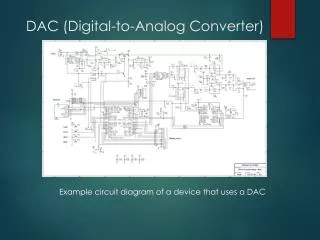
This project summary presents a high-quality digital-to-analog converter (DAC) designed specifically for accurate reproduction in high fidelity audio applications. The converter features a 16-bit resolution, low noise operation, and support for standard sampling rates. Utilizing R-2R ladder architecture with a buffer inserted on the output for low output impedance, the design ensures versatile compatibility across various audio applications. Key elements include a D-flip-flop schematic, voltage reference stability, resistor values optimization, output buffer design, and output filter implementation for noise reduction. The comprehensive design assessment demonstrates successful operation within specified voltage ranges while highlighting room for future enhancements such as increasing resistance values for reduced gate sizes, improving temperature stability, broadening output swing, and minimizing output noise.

E N D
Digital to Analog Converter for High Fidelity Audio Applications Matt Smith Alfred Wanga CSE598A
Project Summary • High Quality Audio Applications • Accurate Reproduction [16 bit] • Low Noise • Versatile • Support for Standard Sampling Rates • Specifications that allow use in Various Audio Applications
R-2R Ladder Architecture * Buffer inserted on output for low output impedance
D Flip-Flop Simulation Results CLK DIN Q QNOT
Pass Switch • NMOS pass transistor only • CMOS Transmission gate not needed because we don’t go near VDD • Sized to allow proper operation
Voltage Reference Results • Circuit modified from Homework #3 (2.5V reference) • Reference output stable down to ~3.3V supply voltage • Temperature varies by 400mV over -40C to 85C (3.2 mV/˚C)
Voltage Reference Results • Power supply rejection ratio is 48dB • LSB accuracy corresponds with 7mV p-p supply noise
Resistor • 50K resistor takes ~1700 um2 • We used values of 50K, 25K, 16K, and 8K • Unexpectedly, resistors ended up being a small portion of our total layout
Output Buffer • Unity gain opamp • Open loop gain = 2560
Output Buffer The high end wasn’t a problem – we wouldn’t go that high But what to do about the low end?
Output Filter This noise is partly an artifact of simulation, but a low-pass filter is a good idea anyway
Layout Bias 0 7 15 8 Opamp Tx_gate (2 huge NMOS) 50K resistor D - Flip Flop
Simulation Results Complete-circuit simulation with top 7 bits active and the rest tied high (This simulation took >15 minutes to run and almost overran my storage space)
Simulation Results • Full-circuit simulation with all 16 bits operating. • LSB increments are 28uV • Noise peaks are 1/4LSB
Design Assessment • Maximum output voltage: 3.441V • Minimum output voltage: 1.604V • Voltage swing: 1.836V • LSB voltage change: 28uV • Calculated and observed agree to +- 0.2uV • Just a little noisy … simulation problem or real?
Future Work / Improvements • Increase resistance values to decrease tx_gate size • Temperature stability (reference) • Wide swing output • Decrease noise on output