Download
1 / 65
670 likes | 707 Views
Explore the fascinating history, invention, and operation of Bipolar Junction Transistors (BJTs). Learn about the achievements and challenges faced by the inventors, the advantages and disadvantages over vacuum tubes, the structure, biasing, and modes of operation. Discover how BJTs revolutionized electronics.

E N D
Bipolar Junction Transistors (BJT) BHAVIN V KAKANI Electronics & Communication Engineering Department IT-NU
First - BJTs The transistor was probably the most important invention of the 20th Century, and the story behind the invention is one of clashing egos and top secret research. Reference: Bell Labs Museum B. G. Streetman & S. Banerjee ‘Solid State Electronic Devices’, Prentice Hall 1999.
Interesting story… Picture shows the workbench of John Bardeen (Stocker Professor at OU) and Walter Brattain at Bell Laboratories. They were supposed to be doing fundamental research about crystal surfaces. The experimental results hadn't been very good, though, and there's a rumor that their boss, William Shockley, came near to canceling the project. But in 1947, working alone, they switched to using tremendously pure materials. It dawned on them that they could build the circuit in the picture. It was a working amplifier! John and Walter submitted a patent for the first working point contact transistor.
Interesting story… Shockley was furious and took their work and invented the junction transistor and submitted a patent for it 9 days later. The three shared a Nobel Prize in 1955. Bardeen and Brattain continued in research (and Bardeen later won another Nobel). Shockley quit to start a semiconductor company in Palo Alto. It folded, but its staff went on to invent the integrated circuit (the "chip") and to found Intel Corporation. By 1960, all important computers used transistors for logic, and ferrite cores for memory.
Point-Contact Transistor – first transistor ever made
Qualitative basic operation of point-contact transistor Problems with first transistor…
First Bipolar Junction Transistors W. Shockley invented the p-n junction transistor The physically relevant region is moved to the bulk of the material
Bipolar Junction Transistors Advantages Of TransistorsOver Vacuum Tubes • Much- Smaller And Lighter • Consume Much less Power • Do Not Get Hot • More rugged – No Glass to Break • No Warm Up Time Needed
Bipolar Junction TransistorsDisadvantages Of TransistorsOver Vacuum Tubes • Can Not Handle Same Amount of Power • Sensitive To Temperature and Radiation • Harder To Mass Produce
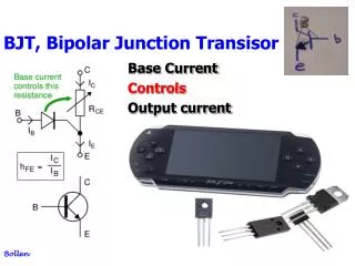
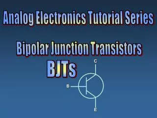
The Structure The Bipolar Junction Transistor (BJT) • Bipolar: both electrons and holes are involved in current flow. • Junction: has two p-n junctions. • Transistor: Transfer + Resistor. • It can be either n-p-n type or p-n-ptype. • Has three regions with three terminals labeled as i. Emitter (E) ii. Base (B) and iii. Collector (C)
Bipolar Junction Transistors Transistor Types • Because there are two junctions, transistors are generally labeled with the prefix “ 2N”: • 2N3904 • 2N3906 • 2N2222 • 2N2907
Bipolar Junction TransistorsTerminals Base Emitter 2N 3904 Emitter Collector Collector Base
force – voltage/current water flow – current - amplification Understanding of BJT
The Structure: npn & pnp • Base is made much narrow. • Emitter is heavily doped (p+, n+). • Base is lightly doped (p-, n-). • Collector is lightly doped (p, n).
Bipolar Junction TransistorsBias • Base • Used to control amount of collector current flow • Changes the “resistance” of the transistor (E to C) • Base-Emitter Junction • Must be Forward Biased! • Base-Collector Junction • Must Be Reverse Biased!
Basic models of BJT npn transistor • Transistors can be constructed as two diodes that are connected together. Diode Diode pnp transistor Diode Diode
Circuit Symbol Layout and Circuit Symbol: n-p-n Transistor • The arrow indicates the direction of current flow. • The current flows from collector to emitter in an n-p-n transistor. • The arrow is drawn on the emitter. • The arrow always points towards the n-type. So the emitter is n-type and the transistor is n-p-n type.
Circuit Symbol Layout and Circuit Symbol: p-n-p Transistor • The arrow indicates the direction of current flow. • The current flows from emitter to collectorin an p-n-p transistor. • The arrow points towards the n-type. • So the base is n-type and transistor is p-n-p type.
Terminal Currents IC Collector current IB Base current IE Emitter current Reference Positive Current Directions 10
Modes of Operation • Based on the bias voltages applied at the two p-n junctions, transistors can operate in three modes: 1. Cut-off (both EB and CB junctions are reversed biased) 2. Saturation (both EB and CB junctions are forward biased) 3. Active mode (EBJ is forward biased and CBJ is reversed biased) • Cut-off and Saturation modes are used in switching operation. • Active mode is used in amplification purposes.
Modes of Operation - VBC + + VBE - Cut-off • Both the junctions are reversed biased. • No current can flow through either of the junctions. • So the circuit is open. Ideal model of BJT in cut-off. 11
Modes of Operation - VBC + + VBE - Saturation: Ideal Model • Both the junctions are forward biased. • So the equivalent circuit can be represented by short-circuit between the base, emitter and collector. Ideal model of BJT in saturation. 12
Modes of Operation Saturation: Practical Model VCE(sat) is in the range of 0.1 to 0.2 V, as VBC and VBE are both approximately equal to the diode forward drop. 13
Active Mode Operation EBJ: Forward Biased CBJ: Reverse Biased • Forward bias of EBJ injects electrons from emitter into base (Emitter current). • Most electrons shoot through the base into the collector (Collector current). • Some emitted electrons recombine with holes in p-type base (Base Current)
Both biasing potentials have been applied to a pnp transistor and resulting majority and minority carrier flows indicated. • Majority carriers (+) will diffuse across the forward-biased p-n junction into the n-type material. • A very small number of carriers (+) will through n-type material to the base terminal. Resulting IB is typically in order of microamperes. • The large number of majority carriers will diffuse across the reverse-biased junction into the p-type material connected to the collector terminal.
Hole electron N P N + - + - + - + - C E + - + - + - + - + - + - B
Electron diffusion Hole diffusion E-Field N P N + - + - C E + - + - + - + - VBE VCB B
E-Field N P N + - + - C E + - + - + - + - Electron hole recombination VBE VCB B
Majority carriers can cross the reverse-biased junction because the injected majority carriers will appear as minority carriers in the n-type material. • Applying KCL to the transistor : IE = IC + IB • The comprises of two components – the majority and minority carriers IC = ICmajority + ICOminority • ICO – IC current with emitter terminal open and is called leakage current.
Collector current Electrons that diffuse across the base to the CBJ junction are swept across the CBJ depletion to the collector because of the higher potential applied to the collector • The equation above shows that the BJT is indeed a voltage-dependent current source; thus it can be used as an amplifier.
Common-Base Configuration • Common-base terminology is derived from the fact that the : - base is common to both input and output of the configuration. - base is usually the terminal closest to or at ground potential. • All current directions will refer to conventional (hole) flow and the arrows in all electronic symbols have a direction defined by this convention. • Note that the applied biasing (voltage sources) are such as to establish current in the direction indicated for each branch.
To describe the behavior of common-base amplifiers requires two set of characteristics: • Input or driving point characteristics. • Output or collector characteristics • The output characteristics has 3 basic regions: • Active region –defined by the biasing arrangements • Cutoff region – region where the collector current is 0A • Saturation region- region of the characteristics to the left of VCB = 0V
The curves (output characteristics) clearly indicate that a first approximation to the relationship between IE and IC in the active region is given by IC ≈IE • Once a transistor is in the ‘on’ state, the base-emitter voltage will be assumed to be VBE = 0.7V
In the dc mode the level of IC and IE due to the majority carriers are related by a quantity called alpha = IC = IE + ICBO • It can then be summarize to IC = IE (ignore ICBO due to small value) • For ac situations where the point of operation moves on the characteristics curve, an ac alpha defined by • Alpha a common base current gain factor that shows the efficiency by calculating the current percent from current flow from emitter to collector.The value of is typical from 0.9 ~ 0.998.
Biasing • Proper biasing CB configuration in active region by approximation IC IE (IB 0 uA)
Common-Emitter Configuration • It is called common-emitter configuration since : - emitter is common or reference to both input and output terminals. - emitter is usually the terminal closest to or at ground potential. • Almost amplifier design is using connection of CE due to the high gain for current and voltage. • Two set of characteristics are necessary to describe the behavior for CE ;input (base terminal) and output (collector terminal) parameters.
Proper Biasing common-emitter configuration in active region
IB is microamperes compared to miliamperes of IC. • IB will flow when VBE > 0.7V for silicon and 0.3V for germanium • Before this value IB is very small and no IB. • Base-emitter junction is forward bias • Increasing VCE will reduce IB for different values. Input characteristics for a common-emitter NPN transistor
Output characteristics for a common-emitter npn transistor • For small VCE (VCE < VCESAT, IC increase linearly with increasing of VCE • VCE > VCESAT IC not totally depends on VCE constant IC • IB(uA) is very small compare to IC(mA). Small increase in IB cause big increase in IC • IB=0 A ICEO occur. • Noticing the value when IC=0A. There is still some value of current flows.