Topic 5 Bipolar Junction Transistors
760 likes | 1.18k Views
ECE 271 Electronic Circuits I. Topic 5 Bipolar Junction Transistors. Chap 5 - 1. Chapter Goals. Explore physical structure of bipolar transistor Understand bipolar transistor action and importance of carrier transport across base region Study terminal characteristics of BJT.

Topic 5 Bipolar Junction Transistors
E N D
Presentation Transcript
ECE 271 Electronic Circuits I Topic 5Bipolar Junction Transistors Chap 5 - 1 NJIT ECE271 Dr. Serhiy Levkov
Chapter Goals • Explore physical structure of bipolar transistor • Understand bipolar transistor action and importance of carrier transport across base region • Study terminal characteristics of BJT. • Explore differences between npnand pnp transistors. • Define four operation regions of BJT. • Explore simplified models for each operation region. • Study Q-point Biasing of BJT. Chap 5 - 2 NJIT ECE271 Dr. Serhiy Levkov
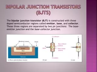
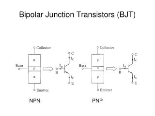
Bipolar Transistor: Physical Structure • Consists of 3 alternating layers of n- and p-type semiconductor called emitter (E), base (B) and collector (C). Chap 5 - 3 NJIT ECE271 Dr. Serhiy Levkov
Bipolar Transistor: Physical Structure • Consists of 3 alternating layers of n- and p-type semiconductor called emitter (E), base (B) and collector (C). • Majority of current enters collector, crosses base region and exits through emitter. A small current also enters base terminal, crosses base-emitter junction and exits through emitter. Chap 5 - 4 NJIT ECE271 Dr. Serhiy Levkov
Bipolar Transistor: Physical Structure • Consists of 3 alternating layers of n- and p-type semiconductor called emitter (E), base (B) and collector (C). • Majority of current enters collector, crosses base region and exits through emitter. A small current also enters base terminal, crosses base-emitter junction and exits through emitter. • Carrier transport in the active base region directly beneath the heavily doped (n+) emitter dominates i-v characteristics of BJT. Chap 5 - 5 NJIT ECE271 Dr. Serhiy Levkov
npn Transistor and pn-junctions • Base-emitter voltage vBE and base-collector voltage vBC determine currents in transistor Chap 5 - 6 NJIT ECE271 Dr. Serhiy Levkov
npn Transistor and pn-junctions • Base-emitter voltage vBE and base-collector voltage vBC determine currents in transistor • They are said to be positive when they forward-bias their respective pnjunctions. Chap 5 - 7 NJIT ECE271 Dr. Serhiy Levkov
npn Transistor and pn-junctions • Base-emitter voltage vBE and base-collector voltage vBC determine currents in transistor • They are said to be positive when they forward-bias their respective pnjunctions. • The terminal currents are collector current(iC ), base current (iB) and emitter current (iE). Chap 5 - 8 NJIT ECE271 Dr. Serhiy Levkov
npn Transistor and pn-junctions • Base-emitter voltage vBE and base-collector voltage vBC determine currents in transistor • They are said to be positive when they forward-bias their respective pnjunctions. • The terminal currents are collector current(iC ), base current (iB) and emitter current (iE). • Primary difference between BJT and FET is that iB is significant while iG = 0. Chap 5 - 9 NJIT ECE271 Dr. Serhiy Levkov
npn Transistor: How it Works (common emitter) • Leftpnjunction is forward biased – open. • Right pnjunction is reverse biased – closed. • If those would be regular diodes – no current would exist btw emitter and collector. • But the width of the base is very narrow, two back-to-back pn junctions are tightly coupled. • Electrons injected from emitter into base region rush through it and are removed by collector, creating collector current IC. • Some of the electrons will travel to the base, creating base current IB . • Base current is usually quite smaller: where bis the common-emitter current gain usually is in the range 50 to 200. • Thus transistor works as a current amplifier: Look for relationship btw iB and iC. Simulation: http://learnabout-electronics.org/bipolar_junction_transistors_05.php Chap 5 - 10 NJIT ECE271 Dr. Serhiy Levkov
npn Transistor: How it Works (common base) • Leftpnjunction is forward biased – open. • Right pnjunction is reverse biased – closed. • Similarly, since the width of the base is very narrow, electrons injected from emitter into the base region rush through it and are removed by collector, creating collector current IC. • Some of the electrons will travel to the base, creating base current IB . • Base current is usually quite small. • Considering transistor as a super node: • where • is common-base current gain. Look for relationship btw iE and iC. Chap 5 - 11 NJIT ECE271 Dr. Serhiy Levkov
npn Transistor Model: Forward Characteristics • BJT is almost symmetrical, except that usually emitter is more heavily doped then collector. • Thus we consider two models: • when BE is forward biased and BC is zero biased (forward characteristics) Chap 5 - 12 NJIT ECE271 Dr. Serhiy Levkov
npn Transistor Model: Forward Characteristics • BJT is almost symmetrical, except that usually emitter is more heavily doped then collector. • Thus we consider two models: • when BE is forward biased and BC is zero biased (forward characteristics) • when BC is forward biased and BE is zero biased (reverse characteristics). Chap 5 - 13 NJIT ECE271 Dr. Serhiy Levkov
npn Transistor Model: Forward Characteristics Forward transport current is Where IS is saturation current VT = kT/q =0.025 V at room temperature • BJT is almost symmetrical, except that usually emitter is more heavily doped then collector. • Thus we consider two models: • when BE is forward biased and BC is zero biased (forward characteristics) • when BC is forward biased and BE is zero biased (reverse characteristics). Chap 5 - 14 NJIT ECE271 Dr. Serhiy Levkov
npn Transistor Model: Forward Characteristics Forward transport current is Where IS is saturation current VT = kT/q =0.025 V at room temperature Base current: is forward common-emitter current gain • BJT is almost symmetrical, except that usually emitter is more heavily doped then collector. • Thus we consider two models: • when BE is forward biased and BC is zero biased (forward characteristics) • when BC is forward biased and BE is zero biased (reverse characteristics). Chap 5 - 15 NJIT ECE271 Dr. Serhiy Levkov
npn Transistor Model: Forward Characteristics Forward transport current is Where IS is saturation current VT = kT/q =0.025 V at room temperature Base current: is forward common-emitter current gain • BJT is almost symmetrical, except that usually emitter is more heavily doped then collector. • Thus we consider two models: • when BE is forward biased and BC is zero biased (forward characteristics) • when BC is forward biased and BE is zero biased (reverse characteristics). Emitter current is given by is forward common- base current gain Chap 5 - 16 NJIT ECE271 Dr. Serhiy Levkov
npn Transistor Model: Forward Characteristics Forward transport current is Where IS is saturation current VT = kT/q =0.025 V at room temperature Base current: is forward common-emitter current gain • BJT is almost symmetrical, except that usually emitter is more heavily doped then collector. • Thus we consider two models: • when BE is forward biased and BC is zero biased (forward characteristics) • when BC is forward biased and BE is zero biased (reverse characteristics). Emitter current is given by is forward common- base current gain In the forward active operation region: Chap 5 - 17 NJIT ECE271 Dr. Serhiy Levkov
npn Transistor Model: Reverse Characteristics Reverse transport current is Chap 5 - 18 NJIT ECE271 Dr. Serhiy Levkov
npn Transistor Model: Reverse Characteristics is reverse common-emitter current gain Reverse transport current is Base current is given by Chap 5 - 19 NJIT ECE271 Dr. Serhiy Levkov
npn Transistor Model: Reverse Characteristics is reverse common-emitter current gain Base currents in forward and reverse modes are different due to asymmetric doping levels in emitter and collector regions. Reverse transport current is Base current is given by Chap 5 - 20 NJIT ECE271 Dr. Serhiy Levkov
npn Transistor Model: Reverse Characteristics is reverse common-emitter current gain Base currents in forward and reverse modes are different due to asymmetric doping levels in emitter and collector regions. Emitter current is given by Reverse transport current is is reverse common-base current gain Base current is given by In the reverse active operation region: Chap 5 - 21 NJIT ECE271 Dr. Serhiy Levkov
pnp Transistor: Structure • Voltages vEB and vCB are positive when they forward bias their respective pn junctions. • Collector current and base current exit transistor terminals and emitter current enters the device. Chap 5 - 22 NJIT ECE271 Dr. Serhiy Levkov
pnp Transistor: Forward Characteristics Base current is given by Emitter current is given by Forward transport current is Chap 5 - 23 NJIT ECE271 Dr. Serhiy Levkov
pnp Transistor: Reverse Characteristics Base current is given by Emitter current is given by Reverse transport current is Chap 5 - 24 NJIT ECE271 Dr. Serhiy Levkov
Operation Regions of Bipolar Transistors Binary Logic States Chap 5 - 25 NJIT ECE271 Dr. Serhiy Levkov
i-v Characteristics of BJT (Recall MOSFET) Chap 5 - 26 NJIT ECE271 Dr. Serhiy Levkov
i-v Characteristics of BJT (npn): Common-Emitter Output Characteristics Circuit to measure output characteristic: For iB= 0, transistor is cutoff. When iB > 0, and increases, iCalso increases. For vCE > vBE, npntransistor is in forward-active region, iC = bFiB is independent of vCE. For vCE< vBE, transistor is in saturation (the voltage btw collector and emitter is small, base collector diode conducts). For vCE< 0, roles of collector and emitter reverse. npn For pnp, iC vs. vEC Chap 5 - 27 NJIT ECE271 Dr. Serhiy Levkov
i-v Characteristics of BJT (pnp): Common-Emitter Output Characteristics Circuit to measure output characteristic: Chap 5 - 28 NJIT ECE271 Dr. Serhiy Levkov
i-v Characteristics of BJT (npn): Common-Emitter Transfer Characteristic Defines relation between collector current and base-emitter voltage of transistor. Almost identical to transfer characteristic of pn junction diode Setting vBC = 0 in the collector-current expression yields Collector current expression has the same form as that of the diode equation Chap 5 - 29 NJIT ECE271 Dr. Serhiy Levkov
Simplified Cutoff Region Model The full BJT model is the so called Gummel-Poon transport model, which is relatively complicated. For our purpose, it will be enough to use the simplified model. Chap 5 - 30 NJIT ECE271 Dr. Serhiy Levkov
Simplified Cutoff Region Model The full BJT model is the so called Gummel-Poon transport model, which is relatively complicated. For our purpose, it will be enough to use the simplified model. In cutoff region both junctions are reverse-biased, transistor is off state: vBE < 0, vBC < 0 If we assume that , where VT = kT/q =0.025 and -4kT/q = -0.1 V, then , and the transport model terminal current equations simplifies: Chap 5 - 31 NJIT ECE271 Dr. Serhiy Levkov
Simplified Cutoff Region Model The full BJT model is the so called Gummel-Poon transport model, which is relatively complicated. For our purpose, it will be enough to use the simplified model. In cutoff region both junctions are reverse-biased, transistor is off state: vBE < 0, vBC < 0 If we assume that , where VT = kT/q =0.025 and -4kT/q = -0.1 V, then , and the transport model terminal current equations simplifies: As will be shown in the example (next slide) those currents are so small that for practical purposes, they are essentially zero. Thus, equivalent circuit: Chap 5 - 32 NJIT ECE271 Dr. Serhiy Levkov
Simplified Cutoff Region Model (Example) • Problem: Estimate terminal currents using simplified transport model • Given data: IS = 10-16 A,aF = 0.95, aR = 0.25, VBE = 0 V, VBC = -5 V • Assumptions: Simplified transport model assumptions • Analysis: From given voltages, we know that transistor is in cutoff. For practical purposes, all three currents are essentially zero. Chap 5 - 33 NJIT ECE271 Dr. Serhiy Levkov
Simplified Forward-Active Region: Model In forward-active region, emitter-base junction is forward-biased and collector-base junction is reverse-biased: vBE > 0, vBC < 0 The simplified transport model terminal current equations: and Conclusion. All currents are independent of the base-collector voltage vBC . The collector current can be modeled as a current source that is controlled by the base-emitter voltage. Chap 5 - 34 NJIT ECE271 Dr. SerhiyLevkov
Simplified Forward-Active Region: Circuit • Current in base-emitter diode is amplified by common-emitter current gain bF and appears at collector; base and collector currents are exponentially related to base-emitter voltage. NL CVD Chap 5 - 35 NJIT ECE271 Dr. Serhiy Levkov
Simplified Forward-Active Region: Circuit • Current in base-emitter diode is amplified by common-emitter current gain bF and appears at collector; base and collector currents are exponentially related to base-emitter voltage. • For simplicity, base-emitter diode can be replaced by constant voltage drop model (VBE = 0.7 V) since it is forward-biased in forward-active region. NL CVD Chap 5 - 36 NJIT ECE271 Dr. Serhiy Levkov
Simplified Forward-Active Region: Circuit • Current in base-emitter diode is amplified by common-emitter current gain bF and appears at collector; base and collector currents are exponentially related to base-emitter voltage. • For simplicity, base-emitter diode can be replaced by constant voltage drop model (VBE = 0.7 V) since it is forward-biased in forward-active region. • Like with the diode, using NL model circuit, requires solving nonlinear diode equation in combination with other equations for the circuit in order to find vBE , iBand iC. or NL CVD Chap 5 - 37 NJIT ECE271 Dr. Serhiy Levkov
Simplified Forward-Active Region: Circuit • Current in base-emitter diode is amplified by common-emitter current gain bF and appears at collector; base and collector currents are exponentially related to base-emitter voltage. • For simplicity, base-emitter diode can be replaced by constant voltage drop model (VBE = 0.7 V) since it is forward-biased in forward-active region. • Like with the diode, using NL model circuit, requires solving nonlinear diode equation in combination with other equations for the circuit in order to find vBE , iB, iC, and iE. • When using CVD model, vBE is postulated as 0.7V, and iB, iC , and iEare found in combination with other equations for the circuit. NL CVD Chap 5 - 38 NJIT ECE271 Dr. Serhiy Levkov
Simplified Forward-Active Region Model (Example 1) • Problem: Estimate terminal currents and base-emitter voltage • Given data: IS =10-16 A,aF = 0.95, VBC = VB - VC = -5 V, IE = 100 mA • Assumptions: Simplified transport model assumptions, room • temperature operation, VT = 25.0 mV Do example on the board Chap 5 - 39 NJIT ECE271 Dr. Serhiy Levkov
Simplified Forward-Active Region Model (Example 1) • Problem: Estimate terminal currents and base-emitter voltage • Given data: IS =10-16 A,aF = 0.95, VBC = VB - VC = -5 V, IE = 100 mA • Assumptions: Simplified transport model assumptions, room • temperature operation, VT = 25.0 mV • Analysis: Current source forward-biases base-emitter diode, VBE > 0, • VBC < 0, we know that transistor is in forward-active operation region. Chap 5 - 40 NJIT ECE271 Dr. Serhiy Levkov
Simplified Forward-Active Region Model (Example 2) • Problem: Estimate terminal currents, base-emitter and base-collector • voltages. • Given data: IS = 10-16 A,aF = 0.95, VC = +5 V, IB = 100 mA • Assumptions: Simplified transport model assumptions, room • temperature operation, VT = 25.0 mV Do example on the board Chap 5 - 41 NJIT ECE271 Dr. Serhiy Levkov
Simplified Forward-Active Region Model (Example 2) • Problem: Estimate terminal currents, base-emitter and base-collector • voltages. • Given data: IS = 10-16 A,aF = 0.95, VC = +5 V, IB = 100 mA • Assumptions: Simplified transport model assumptions, room • temperature operation, VT = 25.0 mV • Analysis: Current source causes base current to forward-bias base-emitter diode, VBE > 0, VBC <0, we know that transistor is in forward-active operation region. Chap 5 - 42 NJIT ECE271 Dr. Serhiy Levkov
Simplified Forward-Active Region Model(Example 3) • Problem: Find Q-point • Given data: bF = 50, bR = 1 VBC = VB - VC = -9 V • Assumptions: Forward-active region of operation, VBE = 0.7 V Do example on the board Chap 5 - 43 NJIT ECE271 Dr. Serhiy Levkov
Simplified Forward-Active Region Model(Example 3) • Problem: Find Q-point • Given data: bF = 50, bR = 1 VBC = VB - VC = -9 V • Assumptions: Forward-active region of operation, VBE = 0.7 V • Analysis: Chap 5 - 44 NJIT ECE271 Dr. Serhiy Levkov
Simplified Reverse-Active Region: Model In reverse-active region, base-collector junction is forward-biased and base-emitter junction is reverse-biased: vBE < 0, vBC > 0 The simplified transport model terminal current equations are: and Conclusion. All currents are independent of the base-collector voltage vBE . The emitter current can be modeled as a current source that is controlled by the base-collector voltage. Chap 5 - 45 NJIT ECE271 Dr. SerhiyLevkov
Simplified Reverse-Active Region: Circuit or • Current in base-collector diode is amplified by the gain bR and appears at collector; base and collector currents are exponentially related to base-collector voltage. CVD NL Chap 5 - 46 NJIT ECE271 Dr. Serhiy Levkov
Simplified Reverse-Active Region: Circuit or • Current in base-collector diode is amplified by the gain bR and appears at collector; base and collector currents are exponentially related to base-collector voltage. • Base-collector diode can be replaced by constant voltage drop model (VBC = 0.7 V) since it is forward-biased in reverse-active region. CVD NL Chap 5 - 47 NJIT ECE271 Dr. Serhiy Levkov
Simplified Reverse-Active Region: Circuit or • Current in base-collector diode is amplified by the gain bR and appears at collector; base and collector currents are exponentially related to base-collector voltage. • Base-collector diode can be replaced by constant voltage drop model (VBC = 0.7 V) since it is forward-biased in reverse-active region. • Like with the diode, using NL model circuit, requires solving nonlinear diode equation in combination with other equations for the circuit in order to find vBC , iB, iCand iE. CVD NL Chap 5 - 48 NJIT ECE271 Dr. Serhiy Levkov
Simplified Reverse-Active Region: Circuit or • Current in base-collector diode is amplified by the gain bR and appears at collector; base and collector currents are exponentially related to base-collector voltage. • Base-collector diode can be replaced by constant voltage drop model (VBC = 0.7 V) since it is forward-biased in reverse-active region. • Like with the diode, using NL model circuit, requires solving nonlinear diode equation in combination with other equations for the circuit in order to find vBC , iB, iCand iE. • When using CVD model, vBC is postulated as 0.7V, and iB, iCand iEare found in combination with other equations for the circuit. CVD NL Chap 5 - 49 NJIT ECE271 Dr. Serhiy Levkov
Simplified Reverse-Active Region: Example • Problem: Find Q-point • Given data: bF = 50, bR = 1 VBE = VB - VE = -9 V. Combination of R and the voltage source forward biases base-collector junction. Do example on the board Chap 5 - 50 NJIT ECE271 Dr. Serhiy Levkov
