Download

1 / 15
150 likes | 318 Views
Nanowires and Nanorings at the Atomic Level. Midori Kawamura, Neelima Paul, Vasily Cherepanov, and Bert Voigtl ä nder. Institut f ü r Schichten und Grenzfl ä chen ISG 3, Forschungszentrum J ü lich, 52425 J ü lich, Germany. Presentation : Kim Jae-Hee. : Ge atom.

E N D
Nanowires and Nanorings at the Atomic Level Midori Kawamura, Neelima Paul, Vasily Cherepanov, and Bert Voigtländer Institut für Schichten und Grenzflächen ISG 3, Forschungszentrum Jülich, 52425 Jülich, Germany Presentation : Kim Jae-Hee
: Ge atom : Si atom Introduction (I-1) • Because most electronics devices are fabricated on Si • substrates, nanostructures grown epitaxially on Si substrates • are most desirable • For the case of the important Si/Ge nanostructure system • the observation of such a growth behavior may not be • observed • In the case of the system Si/Ge it has been difficult to • differentiate between Si and Ge due to their similar electronic • structure. Homogeneous mixed composition [Displacive]
Introduction (I-2) • In a recent approach to distinguish Si and Ge atoms, • a termination of the surface with Cl was used. • this termination of the surface was performed after growth it could not prevent the displacive adsorption of Ge • Si & Ge atoms are located at random locations at the surface in this case.
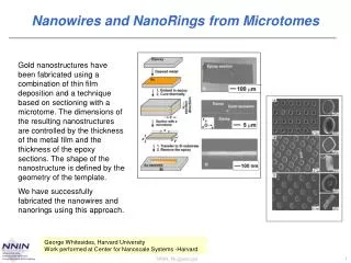
Introduction (II) • The step-growth mode is used to fabricate Si and Ge nanowires • with a width of 3.5nm and a thickness of one atomic layer(0.3nm) by • self-assembly. • Alternating deposition of Ge and Si results in the formation of a • nanowire superlattice covering the whole surface.. • One atomic layer of Bi terminating the surface is used to distinguish between • the elements Si and Ge. • Also, different kinds of two dimensional Si/Ge • nanostructures like alternating Si and Ge nanorings • having a width of 5-10nm were grown
Ge Ge Bi Bi J.H.G. Owen and H.W.Yeom et al, PRL.88, 226104 Introduction (III-1) • Property of Bi : surfactant &.. The property of Bi : surfactant Si
Preexisting step Introduction (III-2) Step-flow growth mode
Si Bi Ge Experiment I 750K 740K 720K Bi, Ge, and Si were deposited on a clean Si(111) substrate by solid source molecular beam epitaxy (MBE). Bi : ~1.000 ML / min Si : ~0.010 ML / min Ge : ~0.015 ML / min STM – home-built beetle-type scanning tunneling microscope sample bias voltage : between +2.2~+2.6V tunneling current : ~ 0.1 nA
STM image of two-dimensional • Ge/Si nanowires grown by step • flow at a preexisting step edge • on a Bi terminated Si(111) • substrate. (c) Atomic structure of a 3.3 nm wide Ge wire on Si substrate capped by Bi ~0.07nm Top view • An STM image after repeated alternating deposition of 0.15 atomic layers of Ge and Si • Both elements can be easily distinguished by the apparent heights in the STM image Side view Initial step position ~3.5nm Final step position Result I Ge Si (b) The cross section along the white line shows the dimensions of the Si and Ge nanowires
Result (I-2) Different width of the wires can be easily achieved by different amounts of Ge and Si deposited. (DC current heating during cleaning of the Si substrate was used) • Si/Ge nanowires on a larger scale • growing at four step edges. • The homogeneity of the nanowires is visible in this STM image. (b) Alternating deposition of nine wires per step edge results in the formation of a superlattice of Si/Ge nanowires covering the whole surface. (~3-5nm wide) 5 3 1 7 6 4 2 8 9 (Ge : 0.1 ML, Si : 0.15 ML)
Template - islands • Substrate – clean Si(111)-7x7 • At 740K, clean surface was initially covered by a one atomic layer • thick Bi layer • Ge and Si deposition of 0.15 ML was performed at T=720 K • and 750 K Experiment - nanorings
~5-10nm 0.09 nm Result II - nanorings
Ge Ge Ge Result II Bi Bi Bi Bi Bi Bi Bi Bi Bi
Analysis Several possible reasons for the observed height difference for Si and Ge areas. (height difference : ~25%) I. • Difference of lattice constant vertical relaxation reliving strain II. Difference surface reconstruction of the terminating Bi layer on Si and Ge Third explanation is confirmed by the fact that the measured height difference shows a pronounced dependence on the applied bias voltage III. Different electron density of states for Bi bond to Si and Ge, respectively
Result III Ge Si Ge Because of Bi trimers Submonolayer Ge deposition on a Sb terminated Si(111) Ge: 0.2 ML Sb : 0.5 ML / min
Summary 1. Control formation of different kind of two-dimensional Si/Ge nanostructure. 2. The property of the nanostructures grown width : 3.5 nm thickness : 0.3 nm cross section consisting of only ~21atoms strong lateral covalent bond 3. A simple and general method has been presented to distinguish between Si and Ge in two-dimensional nanostructures using the height difference in STM images after termination of the surface with Bi