Download
1 / 24
240 likes | 460 Views
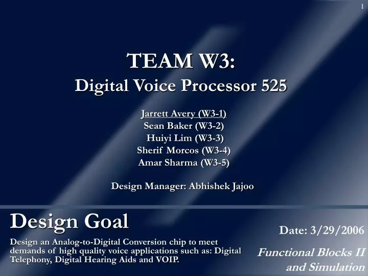
TEAM W3: Digital Voice Processor 525. Jarrett Avery (W3-1) Sean Baker (W3-2) Huiyi Lim (W3-3) Sherif Morcos (W3-4) Amar Sharma (W3-5). Design Manager: Abhishek Jajoo. Design Goal. Date: 3/29/2006 Functional Blocks II and Simulation.

E N D
TEAM W3:Digital Voice Processor 525 Jarrett Avery (W3-1) Sean Baker (W3-2) Huiyi Lim (W3-3) Sherif Morcos (W3-4) Amar Sharma (W3-5) Design Manager: Abhishek Jajoo Design Goal Date: 3/29/2006 Functional Blocks II and Simulation Design an Analog-to-Digital Conversion chip to meet demands of high quality voice applications such as: Digital Telephony, Digital Hearing Aids and VOIP.
Status • Project chosen: 16 bit Delta-Sigma ADC - Basic specs defined • Architecture • Schematic • Floor Planning • Revised Layout Dimensions • Layout Progress • Top Level Analog • Delta/Sigma Modulator • Low Pass Filter – DRC, LVS, Simulated • Top Level Digital • PII – DRC, LVS, Simulated • Sinc Filter – DRC, LVS, Simulated • Clock Divider – DRC, LVS, Simulated • Simulation / Verification • All Digital Modules Verified • All Analog Modules Verified • Overall/Top Verified • Optimized Layout • Analog Components • PII Function – Started Basic Optimization • Sinc Filter
Analog Progress • Delta/Sigma Modulator • Transistor Level Verified with Behavioral • Layouts and Extracted Views of the Operational Amplifiers • Integrator - Verified • Comparator – Verified • Completed DRC/LVS of Module • Common Centriod and MisMatch Analysis • …Working on Analog Top Level Layout • …Begin Schematic/Layout Verification • …Begin Optimizing Module Layout
Delta/Sigma Modulator Transistor Level Simulation Modulator Output Wave Input
Delta/Sigma Modulator Behavorial Level Simulation Modulator Output Wave Input
ΔΣ Modulator Transistor - Layout Comparator Differential Op Amp 17 Analog Transistors
Common Centroid (CC) • Transistor Matching in Analog Design • Concept – Want matched pairs of transistors • (Voltage Matched) Differential Pairs • (Current Matched) Current Mirrors • Common Centroid Layout • Minimize effect of process gradients (ie etching) • Layout style with common center point • Use of “fingers” method most common • Can be used for Matched Resistors/Capacitors
Common Centroid Rules • Coincidence : Centroids of matched devices should coincide • Symmetry : Symmetry should arise from the placement of segments in the array around both the X and Y-axes • Dispersion : Segments of each device should be distributed throughout the array in a uniform manner • Compactness : Array should be as compact as possible and should be nearly square • Orientation : Each matched device should consist of an equal number of segments oriented in either direction (Source: The Art of Analog Layout by Alan Hastings)
Effects of Mismatch on ΔΣ Matched RC and Diff Pair Transistors Increased 10% Diff Pair Size Decreased 10% Diff Pair Size Only 10% RC Mismatch
Sample CC Comparator - Layout R L L R
Digital Progress • Decimator Modules • PII Function - Transistor Level and Layout Verified & LVS • Sinc Filter – Transistor Level and Layout Verified & LVS • Analysis - Power Consumption • Decimator Global Routing • Wired PII, Sinc Filter, and Clock Divider • LVS/DRC of the Decimator Layout • …Decimator to be Simulated • …Some Optimization • Minimize Component (And/Or/Adder) Layouts • Add additional contacts • Connect Nwells, Bigger-Better Vdd, Gnd Lines • Plan Vdd and Gnd Source Grids for Current Distribution • Create Gnd Isolation Rings • …Continue to Optimize PII and Sinc
Sinc (Schematic vs Layout) Schematic Simulation Layout Simulation
PII (Schematic vs Layout) Schematic Simulation Layout Simulation
Decimator – Layout PII Function 256 Clock Divider Sinc2 Filter
Preliminary Top Level - Layout Low Pass Wait Period 1-Bit Stream Min/Max/Out
Problems and Questions • Isolation Rings • How Thick? • Around Analog Modulator? • Around Decimator? • Current Distribution Issues? • Any Comments or Suggestions?