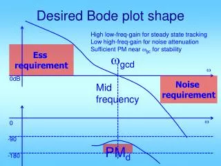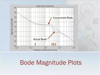
Desired Bode plot shape
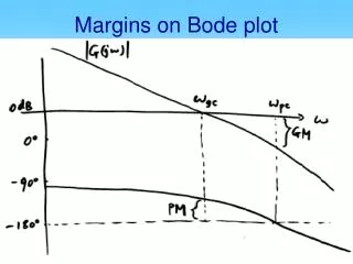
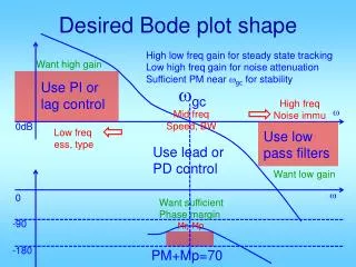
Desired Bode plot shape. High low freq gain for steady state tracking Low high freq gain for noise attenuation Sufficient PM near w gc for stability. Want high gain. Use PI or lag control. w gc. High freq Noise immu. w. Mid freq Speed, BW. 0dB. Low freq ess , type.

Desired Bode plot shape
E N D
Presentation Transcript
Desired Bode plot shape High low freq gain for steady state tracking Low high freq gain for noise attenuation Sufficient PM near wgc for stability Want high gain Use PI or lag control wgc High freq Noise immu w Mid freq Speed, BW 0dB Low freq ess, type Use low pass filters Use lead or PD control Want low gain w 0 Want sufficient Phase margin -90 Mr, Mp -180 PM+Mp=70
Overall Loop shaping strategy • Determine mid freq requirements • Speed/bandwidth wgc • Overshoot/resonance PMd • Use PD or lead to achieve PMd@ wgc • Use overall gain K to enforce wgc • PI or lag to improve steady state tracking • Use PI if type increase neede • Use lag if ess needs to be reduced • Use low pass filter to reduce high freq gain
Proportional controller design • Obtain open loop Bode plot • Convert design specs into Bode plot req. • Select KP based on requirements: • For improving ess: KP = Kp,v,a,des / Kp,v,a,act • For fixing Mp: select wgcd to be the freq at which PM is sufficient, and KP = 1/|G(jwgcd)| • For fixing speed: from td, tr, tp, or ts requirement, find out wn, let wgcd= (0.65~0.8)*wn and KP = 1/|G(jwgcd)|
PD control design Variation • Restricted to using KP = 1 • Meet Mp requirement • Find wgc and PM • Find PMd • Let f = PMd – PM + (a few degrees) • Compute TD = tan(f)/wgcd • KP = 1; KD=KPTD
Lead Design • From specs => PMd and wgcd • From plant, draw Bode plot • Find PMhave = 180 + angle(G(jwgcd) • DPM = PMd - PMhave + a few degrees • Choose a=plead/zlead so that fmax = DPM and it happens at wgcd
Alternative use of lead • Select K so that KG(s) meet ess req. • Find wgc and PM, also find PMd • Determine phi_max, and alpha • Place phi_max a little higher than wgc
Lag and lead-lag Design Steps • From plant, draw Bode plot • From specs => PMd and wgcd • If there is speed or BW req, wgcd, • In this case, if PM not enough, design PD or lead • Otherwise, choose wgcd to have PM>PMd • Find K to enforce wgcd: • Find Kp,v,a-have with K and C above • Find Kp,v,a-des from ess specs • zlag/plag = Kp,v,a-des/Kp,v,a-have • Let zlag= wgcd/5~20, depending on PM room • Compute plag
PI Controller Design Use PI only when you have to increase system type, i.e., when you have to make a nonzero ess to zero!
Gain/Kp In dB Type ↑ LF gain ↑ ess ↓ w=z Let wgc/z big Big phase ↓ Detabilizing w/z
PI controller design • Choice 1: first multiply G by 1/s, then do PD • Choice 2: KP+KI/s=KP (s+z)/s • Do proportional controller design for wgc, PM • Kp • Place zero of PI controller at 10 to 20 times smaller than wgc • z=wgc/(10~20) • KIK=KP z
KI/KP=wgcd/2 KI/KP=wgcd/5 KI/KP=wgcd/10 Want these: DC gain boosting KI/KP=wgcd/20 wgcd KI/KP=wgcd/40 -5.7 -1.4 -2.8 -11.3 -26. 6 Don’t want these: PM reduction! Kill PM significantly
Basic PI Design Steps • From plant, draw Bode plot • From specs => PMd and wgcd • If there is speed or BW req, wgcd, • In this case, if PM not enough, design PD or lead • Otherwise, choose wgcd to have PM>PMd • Find K to enforce wgcd: • Let KP = K • And KI = Kwgcd/10~20, depending on extra PM room to spare Need to increase type to make a nonzero ess to be zero. But no requirement on ess after type increase.
Example Want Mp <= 16% Steady state error = 0 when input is constant. Analysis: steady state error = 0 when input is constant means that ess to step must be 0; or the system type must be 1 or higher. Original system is type 0, so need PI control to increase the system type to 1.
%PI control example n=[500]; d=[1 6 5]; figure(1); clf; margin(n,d); hold on; grid; V=axis; Mp = 16; PMd = 70 - Mp +10; %put in a large extra PM, because PI kills PM semilogx(V(1:2),[PMd-180 PMd-180],':r'); %draw PMd line x=ginput(1); w_gcd = x(1); %get desired w_gc KP = 1/abs(polyval(n,j*w_gcd)/polyval(d,j*w_gcd)); z = w_gcd/10; KI = z*KP; ngc = conv(n, [KP KI]); dgc = conv(d, [1 0]); figure(1); margin(ngc,dgc); grid; [ncl,dcl]=feedback(ngc,dgc,1,1); figure(2);step(ncl,dcl); grid; figure(3); margin(ncl*1.414,dcl); grid;
Ess is 0 Can afford more overshoot!
Sluggish settling is typical of PI or lag controlled systems. Can reduce it by moving the p and z of lag or PI controller to higher frequency.
%PI control example n=[500]; d=[1 6 5]; figure(1); clf; margin(n,d); hold on; grid; V=axis; Mp = 16; PMd = 70 - Mp +10; %put in a large extra PM, because PI kills PM semilogx(V(1:2),[PMd-180 PMd-180],':r'); %draw PMd line x=ginput(1); w_gcd = x(1); %get desired w_gc KP = 1/abs(polyval(n,j*w_gcd)/polyval(d,j*w_gcd)); z = w_gcd/5; KI = z*KP; ngc = conv(n, [KP KI]); dgc = conv(d, [1 0]); figure(1); margin(ngc,dgc); grid; [ncl,dcl]=feedback(ngc,dgc,1,1); figure(2);step(ncl,dcl); grid; figure(3); margin(ncl*1.414,dcl); grid;
PI Design with ess specs • From plant, draw Bode plot • From specs => Kv,a-des, PMd and wgcd • For required ess, Kv,a-des =1/ess • With C(s)=1/s, compute Kv,a-have • If there is speed or BW req, wgcd, • In this case, if PM not enough, design PD or lead • Otherwise, choose wgcd to have PM>PMd • Find K to enforce wgcd: • Let KP = K, KIdes= Kv,a-des/Kv,a-have • If KIdes <= Kwgcd/5~20, done, let KI = KIdes • Else, increase wgcd and go back to previous step Need to increase type by 1 to make a nonzero ess to be zero, and after type increase, there is further requirement on ess.
Example Want Mp <= 16% Steady state error <= 0.1 for ramp input. Analysis: steady state error <= 0.1 for ramp implies that the system type must be 1 or higher. Original system is type 0, so need PI control. Ess to ramp <= 0.1 requires Kvd >= 10. Previous design leaves Kv = KI*500/5 = 100KI = 4.44 KI=0.0444
This is actually the ramp response, generated with the step command but the closed-loop TF is multiplied by 1/s.
In the previous design, KI=0.0444 is already at the maximum of the range Kwgcd/5~20, But KIdes = 0.1, which is a factor of 10/4.44 larger. So need to increase KP. Hence, try letting KI = KIdes = 0.1, and make KP larger by 10/4.44.
Old KI, new KI KP = KP*0.1/KI; KI =0.1; ngc = conv(n, [KP KI]); dgc = conv(d, [1 0]); figure(1); margin(ngc,dgc); grid; [ncl,dcl]=feedback(ngc,dgc,1,1); figure(2);step(ncl,dcl); grid; figure(3); step(ncl,[dcl 0]); grid; Ramp response
PI Design with PD Design Steps • From required ess, Kv,a-des =1/ess • With C(s)=1/s, compute Kv,a-have • Let KI = Kv,a-des/Kv,a-have • Multiply G(s) by KI/s • Do a PD design for KIG(s)/s, with DC gain=1: • Find wgc and PM • Find PMd • Let f = PMd – PM + (a few degrees) • Compute TD = tan(f)/wgcd • KP = KI*TD
%Alternative PI control by PD design clear all; n=[0 0 500]; d=[1 6 5]; ess2ramp = 0.1; Kvd = 1/ess2ramp; Kva = n(end)/d(end); %after introducing 1/s KI = Kvd/Kva; %multiplying G(s) by KI/s and get new Bode ni=KI*n; di=[d 0]; figure(1); clf; margin(ni,di); hold on; grid; [GM,PM,wpc,wgc]=margin(ni,di); PMd=54+6; phi = (PMd-PM)*pi/180; Td = tan(phi)/wgc; KP=KI*Td; ngc = conv(n, [KP KI]); dgc=di; figure(1); margin(n,d); margin(ngc,dgc); [ncl,dcl]=feedback(ngc,dgc,1,1); figure(3);step(ncl,dcl); grid;
clear all; n=[0 0 500]; d=[1 6 5]; ess2ramp = 0.1; Kvd = 1/ess2ramp; Kva = n(end)/d(end); %after introducing 1/s KI = Kvd/Kva; %multiplying G(s) by KI/s and get new Bode ni=KI*n; di=[d 0]; figure(1); clf; margin(ni,di); hold on; grid; [GM,PM,wpc,wgc]=margin(ni,di); PMd=50+3; phi = (PMd-PM)*pi/180; Td = tan(phi)/wgc; KP=KI*Td; ngc = conv(n, [KP KI]); dgc=di; figure(1); margin(n,d); margin(ngc,dgc); [ncl,dcl]=feedback(ngc,dgc,1,1); figure(3);step(ncl,dcl); grid;
Alternative PI Design Steps • For required ess, Kv,a-des =1/ess • With C(s)=1/s, compute Kv,a-have • Let KI = Kv,a-des/Kv,a-have • Rewrite char eq: (KP + KI/s)G(s) + 1=0 • KP*n/d + KI*n/d/s +1 = 0 • KP *n*s + KI*n+d*s =0, KP*n*s/(KI*n+d*s) + 1 =0 • So do a KP design for n*s/(KI*n+d*s), with KI above • Draw Bode plot for n*s/(KI*n+d*s) • Select max PM frequency • Compute KP to make that frequency wgc
%Alternative PI control example clear all; n=[0 0 500]; d=[1 6 5]; %note same length ess2ramp = 0.1; Kvd = 1/ess2ramp; Kva = n(end)/d(end); %after introducing 1/s KI = Kvd/Kva; %get TF after closing the G(s) and KI/s loop ni=[n 0]; di=[d 0]+KI*[0 n]; figure(1); clf; margin(ni,di); grid; x=ginput(1); w_gcd = x(1); %get desired w_gc KP = 1/abs(polyval(ni,j*w_gcd)/polyval(di,j*w_gcd)); ngc = conv(n, [KP KI]); dgc = conv(d, [1 0]); figure(2); margin(n,d); hold on; margin(ngc,dgc); [ncl,dcl]=feedback(ngc,dgc,1,1); figure(3);step(ncl,dcl); grid;