Download
1 / 53
760 likes | 1.12k Views
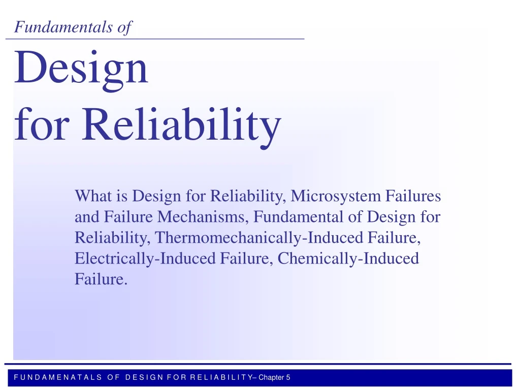
Fundamentals of Design for Reliability. What is Design for Reliability, Microsystem Failures and Failure Mechanisms, Fundamental of Design for Reliability, Thermomechanically-Induced Failure, Electrically-Induced Failure, Chemically-Induced Failure. Introduction.

E N D
Fundamentals of Design for Reliability What is Design for Reliability, Microsystem Failures and Failure Mechanisms, Fundamental of Design for Reliability, Thermomechanically-Induced Failure, Electrically-Induced Failure, Chemically-Induced Failure.
Introduction • Every electronic product is designed to meet four criteria. • Performance • Cost • Size • Reliability • Electrical designers typically design for performance and size. • Manufacturing engineers typically design for cost. • Reliability is not often designed up-front, but rather tested either during the product qualification or after the product is manufactured. • This approach are costly and time-consuming. • The better way is to design for reliability just like for performance, size and cost.
What is Design for Reliability? • When a product performs as designed, it is said to be reliable; when it does not, it is unreliable • Expected lifetime varies • Automobile should last several years and several thousand kilometers • PCs should last 5-7 years • Automotive controller last between 10 and 15 years • Defense electronics should last 30 years • There are two approaches to long-term reliability • Design the package for the desired life - Up-front design needs to identify the potential problems and failure mechanisms, design and select materials and processes that would minimize or eliminate the chances for failure (this is design for reliability) • Perform accelerated test – involves of testing such as thermal cycling, temperature and humidity cycling, power cycling for short period at elevated temperature, higher humidity and so on…….(this is covered in reliability testing)
Microsystems Failures and Failure Mechanisms • The symptoms of failure are often manifest at the systems level (a floppy fails to boot; a TV does not come on; …) • Although these are the high level symptom, but sometimes the failure is really at the lowest hardware level (broken wires; broken joints; …) • All failures are electrical failures eventually, but the causes may be mechanical, thermal, chemical, electrical or a combination of these. • The following diagram outlines 99.9% of the failure mechanisms
Failure Mechanisms in Microsystems Packages • Overstress mechanisms (where stress, in a single event, exceeds the strength or capacity of the component and causes the system failure) • Wear out mechanisms (where failure is gradual and occurs at lower stress levels,repeated application of lower stress over the time results in cumulative damage)
Fundamentals of Design For Reliability • We need to understand the various failure mechanisms (overstress or wear out) in order to design against them • Different mechanisms apply to different applications, and it is often not possible to design against all mechanisms in a given part. • Also, design against one failure mechanism may aggravate a different failure mechanism, thus careful design should be thought to achieve max system level reliability. • We can design against failure by • Reducing the stresses that cause failure • Increasing the strength of the component • This involves • Selecting alternate materials • Changing the package geometry and dimensions. • Introducing new protection or encapsulation • Combination of these methods
Shear stress Compressive stress Definition Strainis defined as the increase in length per unit length of a body subjected to an applied stress. Stress is defined as the applied force per unit area of cross-section of a body. Stress can also be compressive (pushing) or shear, as shown below.
Failure Mechanisms • Typical failure mechanisms in semiconductor packaging are • categorized into few levels – • Die level • Substrate/board level • Interconnect (between die-to -substrate and substrate-to-board) • Assembly/package level
Failure Mechanisms, Accelerating Factors, Designs for Reliability
Themomechanically Induced Failure • These failures result from stresses and strain generated within • electronic package by external or internal heating thermal loading • of the system due to • Mismatch of the thermal coefficient of expansion of the different materials • Thermal gradients in the system • Geometric constraints
Thermomechanical Deformation in Solder Joints When temperature increase from T0 to Tmax, it cause shearing in the solder joints (due to difference in CTE between αb and αc. • αb and αc are the CTE of the board and • the component, respectively, • Three assumption are made • αb > αc , and • assembly does not warp or bend, • Temperature is uniform • then the shearing displacement on the • joints is • L(αb-αc)(Tmax – T0 ) Heating • L(αb-αc)(Tmin – T0 ) Cooling • If the system cycles between Tmax and • Tmin, then the shear stress in a joint of • height h is • γ = ∆ = L (αb –αc)(Tmax – Tmin) • h h • L isDNP (Distance from neutral point)
Maximum Stress at the Edge Due to the DNP (Distance from the Neutral Point) Figure beside illustrate the shear strain point, wherein the max strain is at the outside-edge solder ball where the distance from neutral points (DNP) is maximum.
Design Against Fatigue • Fatigue is the most common mode of failure (90% of all structural and electrical failures) • Fatigue occurs in metals, ceramics and polymers. Ceramics are least susceptible to fatigue failure. • Results of cyclic application of stress; causes dislocations to intersect and create cracks and grow sufficient enough to cause failure example metal paper clip-bend in one direction until it form a sharp kink (this called plastic deformation but does not fracture) then bend it in reverse direction and repeat a few times this paper clip will fracture. • There are two approaches in determining the number of cycles to fatigue failure • High cycle fatigue based on the number of cycle of stress reversals to failure (used in elastic region – macam rubber) • Low cycle fatigue based on strain reversals (used in plastic region or irreversible deformation)
Typical Load Cycle & Endurance Limit Failure does not occur if stress is below the endurance (daya ketahanan) limit, regardless of number of cycles High cycle fatigue is plotted -variation in stress as a function of time. Smax, Smin = max and min stress level ∆S = range of stress (Smax – Smin) Sa = stress amplitude (∆S/2) Nf = Fatigue cycle to failure Smean = Average of max and min stress level Se = endurance limits
Fatigue in Electronic Products • Fatigue occurs in electronic components primarily from power on and power off. • If you turn your PC on and off several times per day (typically about 5), you can generate about 10,000 cycles in about 5 years. • In soldered joints, we usually experience low cycle fatigue because the joints are subject to plastic deformation. • At this stage, you should be able to distinguish between plastic deformation and fracture (ex. Paper clip) Figure shows the example of cracked at solder interconnect.
Crack Cu Crack Propagation in Solder Ball Cu PCB Cu PCB 100 m Crack length 140 m Crack length Crack Initiation
Predictive Fatigue Models • There are four categories of fatigue models for solder joints • Inelastic strain amplitude models (based on Coffin-Manson type fatigue model) • Strain energy density-based Fatigue models • Fracture mechanics-based Fatigue models • Continuum damage mechanics-based Fatigue models
The Coffin-Manson model, applied to most metallic materials in term of plastic strain range, is Where m and C are numerical constants. ∆εp is the plastic strain range (half the plastic strain over one cycle) For solder joint fatigue application, Coffin-Manson is expressed with respect to inelastic shear strain ∆γ, given by: Nf = 0.5 (∆γ/2ε’f)1/c Nf = mean of cycles to failure (fatigue life) 2ε’f = fatigue ductility coefficient c = fatigue ductility exponent (constant) ∆εp = C N Coffin – Manson Low-Cycle Fatigue Model
Effect of Plastic Strain on Fatigue Life As the plastic strain range decrease, the expected fatigue life increase
0.30 0.37 Solomon’s Model Solomon used data from simple shear experiments and determined the low cycle fatigue for Pb-Sn eutectic solders at various temperatures (-50, 35, 125 and 150°C). Solomon’s equation, based on plastic shear strain, is Nf = (θ/∆γp)1/α θ and α are given in table. The average values for the constants θ and α are 1.14 and 0.51 respectively. • There is clearly a temperature dependence of the fatigue life - it decreases with increasing temperature • Note that the authors present a value for θ averaged over all temperatures; this is clearly unprecise formulation (erroneous).
Engelmaier’s Model The C-M type models do not account for the frequency of the fatigue cycle. Engelmaier modified the low cylce fatigue model equation Nf = 0.5 ( ∆γT/2ε’f)1/c c = {-0.442 – [(6 x 10⁻⁴) * Tm]}+ {(1.74 x 10⁻²) * ln (1 + f)} will be given in question Tm = the mean cyclic temperature (°C) = (Tmax. - Tmin) + Tmin. 2 f = the cyclic frequency (1<f<1000 cycles/day) 2ε’f= is the fatigue ductility coefficient ≈ 0.65 IMPORTANT….!!!!
Fatigue Design Guidelines • To reduce strains in solder joints and, therefore improve fatigue life of the solder joints, • we can use the following guidelines. • The CTE of the substrate should be as close as possible to the chip carrier (or the CTE of the chip should be used – in the case of flip chip assemblies) the strain increase with CTE mismatch between the chip carrier and substrate. • Reduce the distance of the joints from the neutral plane; if this is not possible, at least place the most critical joints near the neutral axis the strain typically increase with the distance from the neutral points. • Use designs with excellent thermal paths to reduce both the temperature differences and the temperature gradients, so the heat is easily dissipated strain in solder interconnects increase with ambient temperature condition and with operation temperature gradient. • Use a polymer underfill between the chip and substrate the underfill help to reduce strain in solder joints (as discussed in chapter 4 Flip Chip – underfill is used to compensate the CTE mismatch between the substrate and Si chips. (Other –Polymer Collar and multilayer passivation or structural support layer)
Design Against Brittle Fracture • Brittle fracture is a fracture that occurs rapidly (overstress failure mechanism), with little or no warning when the induced stress exceeds the fracture strength of the material • It occurs in brittle materials such as ceramic, glasses and silicon with little plastic deformation and comparatively little energy absorption. • Ceramic substrates and silicon ICs are candidates for brittle fracture. For brittle material, maximum principle stress is widely used. It failed when the stress reaches a critical value.
Stress-strain Relation of (a) Brittle and (b) Ductile Materials (Fragile) (Deformation similar in plastic material The stress-strain curve is as illustrated; brittle materials exhibit very little (or can consider do not exhibit) plastic deformation prior to fracture.
Brittle Fracture In silicon die, preexisting flaw in the form of a scratch or a nick on the surface that exceeds a critical value under stress conditions causes the die crack. Crack that propagate through the die to an active transistor on the die could leads to device failure. Brittle fracture in most materials is controlled by the presence of cracks or flaws in the material σ = K____ 1.12√πa a = the edge crack depth σ = applied stress K = stress intensity factor (SIF) dependants on the component geometry and loading. Note: that the larger the crack (a), the lower the critical stress for failure
Brittle Fracture Design Guidelines • To minimize the chances of brittle fracture • Brittle fracture is stress controlled. Develop the design (material and processing condition) that minimizes the applied stress • Fracture toughness decreases with surface cracks or flaws in the material. Therefore, prior to assembly, the brittle material should be polished to remove surface flaws and nick.
Design Against Creep-Induced Failure • Creep is a time-dependent deformation of a material under load. • It is thermally activated – stress level increases significantly with temperature. • Material deformation not only dependent to applied load but also dependent on duration and temperature. • In other word, as the load is applied longer (electronic product) – the deformation continues to increase and eventually leads to failure this behavior is called CREEP. • Creep occurs at any stress level, both above and below the yield stress.
Creep Strain vs. Time • There are three stages of creep • Primary, where the creep strain rate decreases rapidly with time • Secondary (or steady-state), where the creep strain rate is constant with time showing a very slow decrease • Tertiary, where the creep strain rate increases rapidly with time, resulting fracture.
Secondary Creep Also known as steady – state creep. In thermomechanical design, it is modeled – constitutes the longest period in the material undergoes before failure. The creep is given by an Arrhenius model (Bevahior for eutectic solder bumps) εc = Aσne-(Q/RgT) As seen, the magnitude of creep strain rate increases with applied stress (σ) and the temperature of the solder joint (T). A = an experimentally determined constand = 1.84 x 10⁻⁴ (MPa)-n (s)-1 n = also experimentally determined = 5.2 Q = activation energy for creep = 50 kJ/mol Rg = universal gas constant = 8.314 x 10⁻³ kJ/mol-K T = temperature of the solder joint in Kelvin (K)
Guidelines to Reduce Creep Induced Failure • To reduce creep-induced failure, we can • Material that has low melting points tend to creep more easily even at room temperature. Use solders with higher melting points, especially for components designed for hash environments (automotive, military) • Creep deformation is dependent to the applied stress, in addition to the operating temperature. Thus reduce the applied mechanical stress • Creep is time controlled phenomenon. The longer a device is exposed to high temperature and high stress, the more creep deformation will be. • Note that for some applications, creep is a not-a critical factor where the expected life is 2-3 years (portable electronic); for others (automotive; aerospace), design to include creep life is a must (critical)
Design Against Delamination Induced Failure • Most packages consist of dissimilar materials that are bonded together • to provide a specific function; • Delamination is the separation or debonding of adjacent layers • There are two types of delamination • Edge delamination • Embedded delamination (occurs in the interior of the package)
Example of Delamination Embedded Delamination in a multilayered structure Edge delamination in flip-chip assembly with underfill
Delamination Effects • Delamination affects circuits in several ways: • Embedded delamination may propagate through metallization to create an open circuit • Edge delamination may reduce mechanical coupling and enhance fatigue • If die attach delaminates there will be reduced thermal cooling, resulting in high junction temperature of the die. • Delamination may results from • Inadequate surface preparation • Inadequate cleaning and presence of contaminants. • Inadequate baking • Moisture and volatile • Inadequate material dispensing. • Non-planarity and topological variation in the surface. • High interfacial stresses.
σxz + σzz≥ 1 σ’xz σ’zz Stress Induced Delamination When the peel stresses and the shear stresses meet the criterion then the delamination will occur. σxz , σzz = shear & peel stress σ’xz , σ’zz = experimental determined shear & peel strength • Once inititated, delamination may or may not propagate, depending on the energy available for it to propagate. • Interfacial fracture mechanics are typically used to predict the propagation of delamination Energy release rate exceed the critical energy release for a given combination of peel and shear mode (delamination will propagate)
Design Against Delamination Failure • To reduce the chances of delamination initiation and delamination, one or more of the • following design guidelines can be used: • Be sure the processing conditions are designed to minimize delamination. Effective process development can help prevent incomplete or inadequate dispensing of encapsulants, underfill or dielectrics and prevent the formation of voids and air bubbles. Baking the organic substrate prior to solder reflow and assembly will drive out moisture and prevent vapor formation. • When is no process induced delamination, reducing the mismatch in engineering properties between adjacent materials can reduce the chances of delamination initiation and propagation. • Improve the adhesion properties between adjacent layers. • Minimize sharp corners in the geometry as sharp corners are potential delamination sites.
Design Against Plastic Deformation • Plastic material - deformation occur when the mechanical stress exceeds the elastic limit or yield points of material. • Elastic material – Vanishes (kembali semula) when the applied load is removed. • Plastic deformation results in a permanent change in the shape of the object • Plastic deformation may not effect the electrical functionality but excessive plastic deformation will ultimately lead to fracture Plastic Deformation
Design Guidelines Against Plastic Deformation • To reduce plastic deformation, one can: • Limit the design stresses to below the yield stress • Select materials with high yield stress • Due to geometrical discontinuities at regions of stress concentrations, or at different material interfaces where stress singularities are present.Be careful with the design of material discontinuities where stress concentrations arise. It necessary to design and control the plastic deformation
Electrically-Induced Failures • All failures in electronic products are electrical failures. • However we should carefully distinguish electrical failure that are mechanically-induced, electrically-induced or chemically-induced and eventually exhibit themselves as electrical failures. • Electrically induced-failures. • Electrostatic discharge • Electromigration • Dielectric breakdown
Electrostatic Discharge (ESD) • Electrostatic discharge (ESD) is the transfer of charge between two bodies at different potentials by direct contact or induced by an electrostatic (electromagnetic) field • Static electricity can also be generated by separating two bodies initially in contact • If the resulting current is not diverted or otherwise handled (by suitable protective mechanism), this transfer of change can • Raise the temperature of the junction inside the component to the melting point • Such temperature raise cause damage to the junction or the connecting lines • The failure can be two types. • Immediate failure: the effects is readily seen • Delayed failure: the device is damaged only up to the point where it may pass the electrical test and QC, but fail early in the product life cycle (intermittent).
Design Guidelines Against ESD • To reduce the chances of ESD. • Provide assembly workstations with conductive floor mats, grounded wrist bands, and conductive table mats as these protects the components from damage due to ESD charge on the body. • Use air ionizers in ESD protective areas, as the ionizers neutralize static charge on non-conductive materials • Ground all test and soldering equipment • Use antistatic foams for storing and shipping components • Measure and control static on components with various meters like electrostatic alarms, electrostatic voltmeters and field meter.
Design Against Gate Oxide Breakdown • An electrical short between the gate metallization and the channel of a MOSFET destroys the operation of the device and is called gate oxide breakdown • Gate Oxide breakdown may result from • Process: defects in the materials resulting from processing may lead to thin oxide regions with higher field strengths • Particles: radiation damage • Process defects are increasingly important as gate oxide gets thinner with faster, thus generate higher electric field. If electric field higher than dielectric breakdown strength can result in failure. • The thinner oxides of modern processes aggravate this problem and increase the electric field across the oxide, further reducing its life time. • To maintain electrical fields below the critical value for dielectric breakdown, the power supply voltage is being reduced • Accidental discharges (ESD) can cause catastrophic failure
Design Against Electromigration • Electromigration is an atom flux induced in metal traces by high current densities. • Atoms in the metal traces see an “electron wind” that helps move atoms (diffusion) in the direction of the electron flow (dislodged from their position) • This causes formation of metal voids, and as this process continues, the resistance drop across the conductor increase, leading eventually to electrical opens. • The increased resistance cause signal speed degradation or even catastrophic failures in the devices. • Electromigration is also detrimental to the life of electronic products and is a reliability issues. • The effect was first observed in 1961 by Blech and Sello
Electromigration Damage Figure depicts an SEM image of metal trace before and after electromigration has taken place. The ion flux generated due to the high current density has caused an electrical open in the circuit.
Design Guidelines Against Electromigration • Electromigration may be reduced by • Electromigration has been mostly noticed in aluminum and silver metallization. Copper traces are found to be more resistant. Al(Cu) alloys also good. • Using shorther traces help the electromigration problem. However, it adds more routing layer and thus more complexity in fabrication. • The effect of electromigration can be controlled by tightly enforcing the current density design rules based on electromigration data.
Chemically-Induced Failure • There are three chemically driven processes that can lead to • cracking/failure of the package • Electrochemical reactions (corrosion) • Diffusion of material • Dendritic growth (saliran bentuk ranting ) • The reactions are often aggravated by increased temperature, increased • voltage and increased thermally
Corrosion Induced Failure • Electrochemical reactions cause gradual depletion of metal in the presence of an electrolyte • These reactions are described in terms of an electrochemical cell which has both an anodic reaction and a cathodic reaction • In the anodic reaction, the metal is oxidized (in the presence of electrolyte) (where electron of metal ions are released) • M M++ + 2e- • M = metal atom M++ = positive ion e- = electron • There is an oxidation potential E associated with the reaction • The positive ions dissolve in the electrolyte. Such dissolution of metal ions gradually depletes the metal.
Corrosion Induced Failure • The electrons combine with specific constituents (such as hydrogen ions) in a cathodic reaction • E = 0 • 2H+ + 2e- H2 (gas)↑ • For this corrosion to occur, there must be • An electrolyte to facilitate the anodic reaction that result in depletion of the metal • A favorable cathodic reaction that absorbs the released electron
Design Guidelines to Reduce Corrosion • Pick materials with low oxidation potentials. Metal that have high oxidation potential tend to corrode faster. Al, Ti and Ni tend to corrode more easily due to their high oxidation potential. “Noble” metal such as Au and Pt more stable. Material rank from most stable to the least stable. • Au, Pt, Ag, Cu , W, Ni, Ti, Al • For corrosion to occur, there needs to be moisture. Use hermetic packages to prevent moisture absorption. Although plastic packages or molding compound cannot prevent moisture absorption, they can prevent contaminants from reaching the critical devices. • Be sure there is no trapped moisture during processing and assembly. Can be achieved by performing assembly in cleanrooms, proper monitoring of contaminant in the assembly area and rinsing the components with deionized water prior assembly.
Design Against Intermetallic Diffusion • Intermetallic diffusion is a common failure mode in electronic interconnections (wirebonds and solder joints) • During wirebonding or solder reflow, the joining process generates intermetallic layers or intermetallic compounds (IMC) which are by-products of the joining process. • The IMC layer is necessary for a good interconnection joint, but too much the IMCs layer formation can lead to local embrittlement and degradation of the mechanical strength.