Download
1 / 41
410 likes | 538 Views
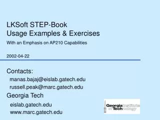
LKSoft STEP-Book Usage Examples & Exercises With an Emphasis on AP210 Capabilities 2002-04-22. Contacts: manas.bajaj@eislab.gatech.edu russell.peak@marc.gatech.edu Georgia Tech eislab.gatech.edu www.marc.gatech.edu. Context.

E N D
LKSoft STEP-Book Usage Examples & ExercisesWith an Emphasis on AP210 Capabilities2002-04-22 Contacts: manas.bajaj@eislab.gatech.edu russell.peak@marc.gatech.edu Georgia Tech eislab.gatech.eduwww.marc.gatech.edu
Context • This assumes you have obtained STEP-Book for AP210 from LKSoft (www.lksoft.com) and have installed it in the default location. It may include others, too, like STEP-Book AP203 • This documentation was tested using this alpha version: • JSDAI v3.0.1a2 (dated 2002-04-17) • Note: screen shots may vary slightly (some are from early versions) • This documentation is a user-oriented supplement to their existing online documentation. It emphasizes illustration of AP210 capabilities • See first the following prerequisites: • General STEP-Book Usage • Start Menu, LKSoft-JSDAI, STEP-Book Documentation
STEP-Book Usage Hints • In 2D/3D geometry shape view windows: • Zoom: Right-Button and move mouse • Pan: Shift-Left-Button and move mouse • Rotate (3D): Left-Button and move mouse • Sometimes after a mouse single-click or double-click, there may be a ~5-10 sec delay on some responses (an hour glass may not show - example during Import) • Sometimes the back button does not behave as expected (go back to the Core Concepts and select again if necessary - the 2D/3D shape you previously selected will still be there) • You cannot have more than one model loaded at a time • Sometimes you may have to exit and re-start to load in a new model • See other known caveats described in these Release Notes • Start Menu, LKSoft-JSDAI, STEP-Book Known Problems
Examples included in STEP-Book • For other STEP model examples, see also: • www.cax-if.org (ap203) • www.ap210.com • Includes examples showing same design in EAGLE ECAD tool and StepBook • pdm-if.org (pdm_schema) • etc.
Contents • AP210 Examples • hexapod.210 • Translated from the common example in the EAGLE ECAD tool • Interconnect-PCB Design View • 2D layout (bare board - including table of traces) • Interconnect-PCA Design View • 2D layout (including table of components) • H08-Package.210 • Package view • 3D, … feature table, seating plane, … • flasher_3D.210 • Includes both 2D and 3D PCA shape views • demo2.210 • Interconnect-PCB Design View • physical network join relationships
Contents (continued) • AP210 Examples - continued • Other electronic component examples • AP203 Examples • Dual in Line Package • 3D Substrate and Socket View • allied_203.203 - Mechanical Part • 3D View • Tool Usage Quiz - AP210 Exercises • demo2.210 • Land patterns, physical networks, passage technologies, … • Documents • flasher_3D.210 • Example end user queries
AP210 Interconnect-PCB Design Viewpca: hexapod.210 aspect: overview of features 3 1 2 (double-click here, then select 2D shape/geometry view) Follow these steps to see the indicated aspects
AP210 Interconnect-PCB Design Viewpca: hexapod.210 aspect: 2D view of traces/features 4 - View table of traces, etc.
AP210 Interconnect-PCB Design Viewpca: hexapod.210 aspect: table of traces (“components”) 6 (zoom) 5a (select a row - can also add/remove/re-arrange table columns) 5b (selected trace is auto-highlighted)
AP210 Interconnect-PCB Design Viewpca: hexapod.210 aspect: selected feature (land) 7 - Can also double-click features in left pane to see their details above
AP210 Interconnect-PCB Design Viewpca: hexapod.210 aspect: list of stratums (layer stackup)
WIP Extension: Stackup OEM View Smart Figure AP210 Interconnect-PCB Design Viewpca: hexapod.210 aspect: list of stratums (layer stackup) Target smart figure illustrating idealized meaning of above attributes
AP210 Interconnect-PCB Design Viewpca: hexapod.210 aspect: stratum feature details (in TopLayer)
AP210 Interconnect-PCB Design Viewpca: hexapod.210 aspect: passage technology (via/pth template) pth = plated-through hole
WIP Extension: Via/PTH Template Smart Figure AP210 Interconnect-PCB Design Viewpca: hexapod.210 aspect: passage technology (via/pth template) Target smart figure illustrating idealized meaning of above attributes pth = plated-through hole
AP210 Assembly-PCA Design View pca: hexapod.210 aspect: overview of features 4 2 3 1
AP210 Assembly-PCA Design Viewpca: hexapod.210 aspect: view selected component - C1 5a (select a component) 5b (selected component is auto-highlighted)
AP210 Assembly-PCA Design Viewpca: hexapod.210 aspect: view selected component - board 6 (board/PCB is also a selectable “component”)
AP210 Package View (Component)component: H08-Package.210 aspect: overview of attributes 4 2 1 3
Contents • AP210 Examples • hexapod.210 • Translated from the common example in the EAGLE ECAD tool • Interconnect-PCB Design View • 2D layout (bare board - including table of traces) • Interconnect-PCA Design View • 2D layout (including table of components) • H08-Package.210 • Package view • 3D, … feature table, seating plane, … • flasher_3D.210 • Includes both 2D and 3D PCA shape views • demo2.210 • Interconnect-PCB Design View • physical network join relationships
AP210 Package View (Component)component: H08-Package.210 aspect: 3D shape 5 See also: video clip http://www.ap210.com/video/package.rm
AP210 Package View (Component)component: H08-Package.210 aspect: list of features 5b (selected smart feature = tab) The 3D shape is generated from these “smart features”. Thus, the 210-based model is much richer than a typical 3D MCAD package model. 210 can also support the detailed design of a package itself (its insides, including electrical functions and physical behaviors).
AP210 Package View (Component)component: H08-Package.210 aspect: seating plane 3 • See also video overview of AP210 support for electronic packages (using this example): • http://www.ap210.com/video/package.rm (7Mb)
Contents • AP210 Examples • hexapod.210 • Translated from the common example in the EAGLE ECAD tool • Interconnect-PCB Design View • 2D layout (bare board - including table of traces) • Interconnect-PCA Design View • 2D layout (including table of components) • H08-Package.210 • Package view • 3D, … feature table, seating plane, … • flasher_3D.210 • Includes both 2D and 3D PCA shape views • demo2.210 • Interconnect-PCB Design View • physical network join relationships
AP210 Assembly-PCA Design Viewpca: flasher_3D.210 aspect: 3D PCA Assembly
AP210 Assembly-PCA Design Viewpca: flasher_3D.210 aspect: 2D PCA Assembly Note that both a 2D and a 3D shape are included in this design model (illustrating support for multiple fidelities of viewpoint).
Contents • AP210 Examples • hexapod.210 • Translated from the common example in the EAGLE ECAD tool • Interconnect-PCB Design View • 2D layout (bare board - including table of traces) • Interconnect-PCA Design View • 2D layout (including table of components) • H08-Package.210 • Package view • 3D, … feature table, seating plane, … • flasher_3D.210 • Includes both 2D and 3D PCA shape views • demo2.210 • Interconnect-PCB Design View • physical network join relationships
AP210 Interconnect-PCB Design Viewpca: demo2.210 aspect: physical network Selected physical network (composed of multiple vias, pads, and traces) on right is highlighted here.
AP210 Interconnect-PCB Design Viewpca: demo2.210 aspect: physical network joins & terminals a. Join relationship on right is highlighted here. b. Double-click above row to see details as given here.
Contents (continued) • AP210 Examples - continued • Other electronic component examples • AP203 Examples • Dual in Line Package • 3D Substrate and Socket View • allied_203.203 - Mechanical Part • 3D View • Tool Usage Quiz - AP210 Exercises • demo2.210 • Land patterns, physical networks, passage technologies, … • Documents • flasher_3D.210 • Example end user queries
AP210 Package View (Component)component: PLCC20 in texas.p21 aspect: part features
AP210 Package View (Component)component: PLCC20 in texas.p21 aspect: 2D shape
AP210 Package View (Component)component: PQFP144 in texas.p21 aspect: 2D shape
Contents (continued) • AP210 Examples - continued • Other electronic component examples • AP203 Examples • Dual in Line Package • 3D Substrate and Socket View • allied_203.203 - Mechanical Part • 3D View • Tool Usage Quiz - AP210 Exercises • demo2.210 • Land patterns, physical networks, passage technologies, … • Documents • flasher_3D.210 • Example end user queries
Dual-in-Line Packagedip-14-socket.203 Substrate and Socket View
Contents (continued) • AP210 Examples - continued • Other electronic component examples • AP203 Examples • Dual in Line Package • 3D Substrate and Socket View • allied_203.203 - Mechanical Part • 3D View • Tool Usage Quiz - AP210 Exercises • demo2.210 • Land patterns, physical networks, passage technologies, … • Documents • flasher_3D.210 • Example end user queries
STEP-Book AP210 Tool Usage Quiz(Optional Hands-on Exercises) Contact russell.peak@marc.gatech.edu if you would like to check your answers.
demo2.210 - PCB aspects Use STEP-Book to find these answers for the above model file. Indicate the user interface path you used to find the main source of information. • How many conductive layers are there in this PCB? • Find the TAP5-45 land pattern “product” • What is its id value? • Draw its design view shape • Find physical network PN-402 (a PCB Design View concept) • Draw its shape and approximate position on the PCB • Label your drawing to show the associated joins with their type and id • Find passage technology PT3 (a characteristic board aspect) • What is its material? • What is the minimum deposition thickness?
demo2.210 - PCA & misc. aspectscontinued • Find the component occurrence with reference designator C4 • Draw a picture to indicate its location on the board and its approximate 2D shape • What is the identifier and publisher for the single document represented in this model?
flasher_3D.210 - PCA aspects • Find the 3D usage view of the PCA • How many components are on the top? • How many are on the bottom? • How many holes (passage components) are visible in this view? • What type attribute value do these passage components have? • Explore other features on your own (e.g., follow connectivities) • Bonus credit: • Obtain 210 Viewer (by Mike Keenan @ Boeing) • View above and: • Determine their position (x, y, side) • Change values and see them move • Other 210 models include “keep out / restricted” regions you can visualize and see