Download
1 / 18
180 likes | 207 Views
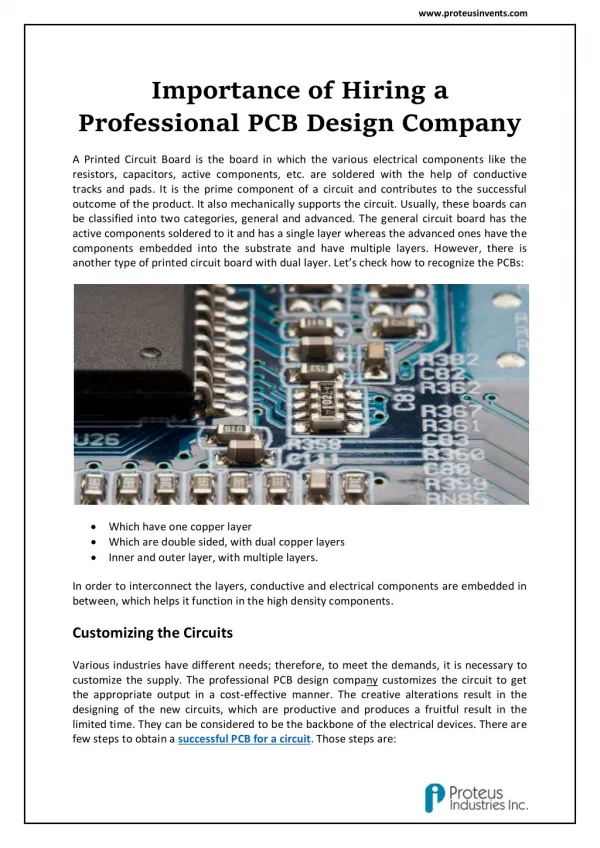
We use Printed Circuit Boards (PCB) for connecting electronic components by using conductive tracks. This allows for prototyping electric circuits and manufacturing electronic products. Mass-production of electronic products based on PCBs is faster and economical as compared to the ones based on alternative wiring techniques. Because in PCBs, components are mounted and wired simultaneously. Therefore, we have to make the PCB layout only onceu00a0andu00a0we can manufacture a large number of PCBs at the same time.<br>

E N D
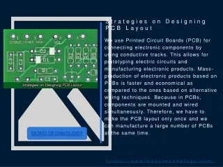
Strategies on Designing PCB Layout We use Printed Circuit Boards (PCB) for connecting electronic components by using conductive tracks. This allows for prototyping electric circuits and manufacturing electronic products. Mass-production of electronic products based on PCBs is faster and economical as compared to the ones based on alternative wiring techniques. Because in PCBs, components are mounted and wired simultaneously. Therefore, we have to make the PCB layout only once and we can manufacture a large number of PCBs at the same time. MOKO TECHNOLOGY https://www.mokotechnology.com/
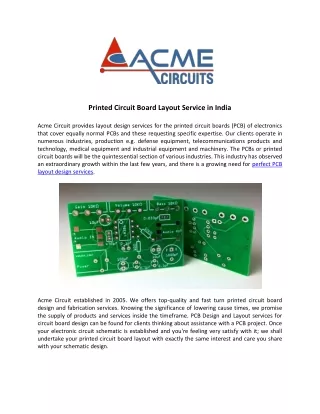
Why PCB Layout is Needed • When it comes to PCBs, designing the Layout is the most important part as it will determine the placement of various components and their resultant roles in the desired product. This guide will explain the process of designing a PCB layout and how you can use it for manufacturing PCBs. • First, we are going to take a look at some of the strategies which are widely used in designing a PCB Layout; 1 3 https://www.mokotechnology.com/ 4
Strategies on Designing PCB Layout https://www.mokotechnology.com/
Strategies on Designing PCB Layout It is a good practice to make a schematic of the circuit before starting the designing of the PCB. The schematic will act as a blueprint for placing components and laying out the traces on the PCB. If you use an efficient PCB designing software then it will allow you to import this schematic and this will make the PCB design process relatively easier. Once you have imported this schematic into an intelligent PCB design software, you can start placing components, wires, and footprints. Once we have done this, we can start designing the PCB layout. https://www.mokotechnology.com/
Reflow Soldering Stage in PCB manufacturing Compartmentalization is a great strategy for designing a PCB layout. We need to identify what is the role of each part of the circuit and then divide the circuit into small sections according to their function. It will help with better visualization of the circuit. You need to keep the components of each section grouped together in the same region of the PCB. This will help in keeping the conductive traces short. It is important as long traces can pick up electromagnetic radiation which may lead to noise and interference. You should arrange various sections of the circuits in such a way that the Compartmentalization is a great strategy for designing a PCB layout. We need to identify what is the role of each part of the circuit and then divide the circuit into small sections according to their function. It will help with better visualization of the circuit. You need to keep the components of each section grouped together in the same region of the PCB. This will help in keeping the conductive traces short. It is important as long traces can pick up electromagnetic radiation which may lead to noise and interference. You should arrange various sections of the circuits in such a way that the power supplied to each section has equal voltage. We call this “star configuration” and it helps in accomplishing shorter traces. https://www.mokotechnology.com/
Reflow Soldering Stage in PCB manufacturing https://www.mokotechnology.com/
Single-layer and Multi-layer Approach You may find it difficult to design large circuits on a single layer PCB. This is because it is difficult to avoid intersection while routing traces. You may need two or more layers with traces routed on multiple sides of the PCB. You can connect traces on one layer to the other layer by using a “via”. We know “via” as a copper-plated hole in a PCB that electrically connects the bottom layer to the top layer. You can also connect the bottom and top traces by using the “through-hole” of the deployed electronic components. https://www.mokotechnology.com/
The 45o Bending technique https://www.mokotechnology.com/
The 45o Bending technique A good practice to design PCBs is to bend most of the copper traces at 45° angles. This is because the 45° angles shorten the electrical path between various components as opposed to the 90° angles. On top of that, high-speed logic signals might get reflected off at sharp angles (close to 90°) which may lead to interference. https://www.mokotechnology.com/
Some Common Mistakes to Avoid in PCB Layout Here are some of the most common mistakes during PCB Layout and how you can avoid them. Choice of Wrong Designing Tool For designing an efficient PCB, it is empirical to choose the right tool. If you choose a wrong or inappropriate tool for PCB designing then it will cause problems such as increased manufacturing costs and extended delay times. Hence, we strongly recommended choosing the appropriate tool which best meets your PCB designing needs. There are a lot of options to choose from and you must do proper homework and research before investing in a certain tool. https://www.mokotechnology.com/
Some Common Mistakes to Avoid in PCB Layout Incompetent Layout Techniques PCB designs are often complex because we often use them to make faster and smaller electronic devices. There is an increasing demand for electronic circuits with minimal footprints. That is why we intend to make PCBs with smaller components that have a reduced footprint. If you choose an incompetent or inappropriate layout technique then the connections might not work properly. If you are working with components with a higher pin-count and a smaller pitch then it is crucial to choose a competent layout technique. https://www.mokotechnology.com/
Some Common Mistakes to Avoid in PCB Layout Improper Thickness of Copper The thickness of copper plays an important role in tracing and consequently in PCB designing. If the thickness isn’t adequate then there will be insufficient plating in the holes. That is why it is important to achieve the accurate thickness of copper if you want to attain a good PCB design. Incorrect Placement of Decoupling Capacitors We use decoupling capacitors for maintaining a stable voltage. We often place these capacitors on the power supply rail. We should deploy these capacitors near the pin which needs stable voltage. Decoupling capacitors won’t work properly if they are placed away from the pin which requires stable voltage. https://www.mokotechnology.com/
Some Common Mistakes to Avoid in PCB Layout Failure to Make Backups of Your Work We use different data sets and software for making efficient PCB designs. Due to the various tools involved, the data might get misplaced or permanently lost if you don’t save it after regular intervals. You should make multiple backups of your work so that even if one gets corrupted, the others are still safe and secure. Lack of Design Reviews One of the most essential elements in a PCB design is reviewing the interconnection of the circuits and the functioning of the PCB. Design reviews help in preventing all kinds of design mistakes. People have a certain bias when they are reviewing their own work that is why you must have other people review the PCB design as they might come across some mistake that you might have missed. https://www.mokotechnology.com/
Some Common Mistakes to Avoid in PCB Layout Lack of Communication Stress, multitasking, and fatigue are commonly observed when we are mass-producing PCBs. These factors can lead to miscommunication, which might in turn cause increased cost and operation time. If you want to avoid this then you should ensure good communication across all channels. This will help in designing and manufacturing efficient PCBs that meet your desired service requirements. https://www.mokotechnology.com/
PCB Design Tools There are numerous PCB Layout Design Tools available in the market today. You need to carefully take an objective look at all the major ones and then choose the right tool which meets all of your needs. Here are some of the layout design tools which are widely used in the PCB industry. ZenitPCB It is a great software tool for creating amazing PCB layout designs. It is very easy to use and is very flexible. This CAD program enables its users to realize the projects in a very short time. ZenitPCB makes it possible to create the project by starting from the layout directly or by first making a schematic. Osmond PCB Osmond PCB is a flexible tool for designing PCB layouts. It features a number of board layers and parts, virtually unlimited board sizes, support for surface-mounted and through-hole parts. https://www.mokotechnology.com/
PCB Design Tools ExpressPCB Easy to use and learn. This software makes it very easy to design PCB layouts even if the user is a beginner or doesn’t have any prior knowledge. Kicad This tool helps in making electronic schematic diagrams and PCB layouts. It supports designing layouts of PCBs with up to 16 layers. gEDA It has features that allow for schematic capture, prototyping, production, and simulation. It offers a mature suite for PCB layout design, attribute management, BOM generation, electronic design, netlisting, and analog & digital simulation. https://www.mokotechnology.com/
PCB Design Tools DesignSpark PCB This tool has the highest accessibility when compared to other electronic design tools. It is very easy to use and yet easier to learn. Experts use this tool to reduce turnover times. This tool has a powerful design engine which makes it very convenient to design PCB layouts, boards, and schematics. TinyCAD This program helps in drawing detailed circuit diagrams. It has built-in symbol libraries that help in getting started right away. This tool also allows for simple printing of PCB designs. It has universal publishing features that provide support across multiple platforms. Hence, this tool offers excellent integration and customization. https://www.mokotechnology.com/
MOKO Smart is a renowned name when it comes to PCB Designing and manufacturing. MOKO Smart uses cutting edge tools for designing its PCB layouts and we can help you with designing layouts that meet your specific needs. We have a very sophisticated setup for manufacturing its premium quality PCBs. If you have managed to come up wit brilliant single-layered or multi-layered PCBs but can’t manage to realize your conceptualization then you don’t need to worry as MOKO Smart has got you covered. All you need to do is to reach out to us and we will take it from there. Hoping to hear from you soon! MOKO TECHNOLOGY