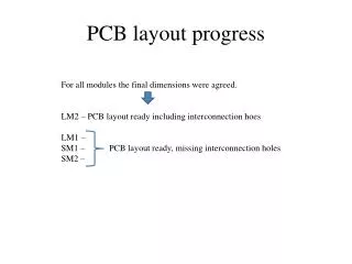
PCB layout progress
PCB layout progress. For all modules the final dimensions were agreed. LM2 – PCB layout ready including interconnection hoes LM1 – SM1 – PCB layout ready, missing interconnection holes SM2 – . Interconnection holes – LM2. PCB edge. Eta. Stereo. Interconnection holes – LM2.

PCB layout progress
E N D
Presentation Transcript
PCB layout progress For all modules the final dimensions were agreed. LM2 – PCB layout ready including interconnection hoes LM1 – SM1 – PCB layout ready, missing interconnection holes SM2 –
Interconnection holes – LM2 PCB edge Eta Stereo
Interconnection holes – LM2 360 360 360 360 350 350 350 350
4 different solutions CERN – LM2 Saclay – LM1 LNF – SM1 LMU – SM2
PCB cut-out Present version New version?
Proposal for spacer/mesh frame 30 14 6 8 2 7 Glue O-ring 5.00* 5 + δ 4.5 5.00* – Drift space δ = 0.06 mm (coverlay) + 0.128 (pillar) ≈ 0.2 mm