Download
1 / 38
380 likes | 572 Views
EET 2261 Unit 8 System Clocks; Seven-Segment Displays; S19 Records. Read Almy , Section 16 and Appendix B. Homework #8 and Lab #8 due next week. Quiz next week. Review: HCS12 Block Diagram.

E N D
EET 2261 Unit 8System Clocks; Seven-Segment Displays; S19 Records • Read Almy, Section 16 and Appendix B. • Homework #8 and Lab #8 due next week. • Quiz next week.
Review: HCS12 Block Diagram • Up to now we’ve focused on the HCS12’s central processing unit (CPU12 in the block diagram on page 6 of textbook or page 23 of Device User Guide). • We’ve also looked at the memory blocks (Flash, RAM, EEPROM). • And we’ve looked at the general-purpose I/O ports (PTA, PTB, etc. in the diagram).
Review: HCS12 Block Diagram • In coming weeks we’ll study other hardware “blocks” (or subsystems) in the HCS12, such as: • Clock and Reset Generator Block • Enhanced Capture Timer Block • Interrupt Block • Up to now our primary reference guide has been the CPU reference manual, but now we’ll need the reference guides for the other blocks, listed here.
Review: Special-Function Registers • Recall that the HCS12 has hundreds of special-function registers. • Most of these registers are either: • Data registers, which transfer data from place to place. (Example: PORTA) • Control registers, which control various aspects of the chip’s operation. (Example: DDRA) • Status registers, which hold status information about events that have occurred.
Review: How to Access the Special-Function Registers • In the HCS12’s memory map (page 26 of Device User Guide), addresses from $0000 to $03FF are assigned to the special-function registers. • When you execute an LDAA or STAA instruction to one of these addresses, you’re not reading or writing to memory; instead, you’re reading from or writing to a special-function register.
Review: List of Special-Function Registers • Pages 27-49 in the Device User Guide list all of the special-function registers and their addresses.
Finding Details on the Special-Function Registers • Up to now the only special-function registers we’ve used are the ones associated with I/O ports, such as PORTA, DDRA, etc. • In coming weeks we’ll discuss many more special-function registers, which are associated with individual hardware blocks. • For details on how these registers are used, refer to the block user guides.
Finding Details on the Special-Function Registers: Example • Example: The register at address $0034, named SYNR, is one of many associated with the Clock and Reset Generator. • For details on this register, refer to p. 15 of the Clock and Reset Generator Block User Guide.
Clock and Reset Generator (CRG) Block • Next we’ll look at the Clock and Reset Generator block, which includes an important circuit called a Phase-Locked Loop (PLL). • Figure from p. 6 of textbook or p. 23 of Device User Guide).
Overview: Clock and Reset Generator (CRG) Block • As its name suggests, this hardware block has two major responsibilities: • Generating the HCS12’s clock signals • Resetting the HCS12 under certain conditions. • See block diagram on p. 11 of the CRG Block User Guide.
Reset Generator • Four conditions can cause the system to reset itself: • Applying power to the chip’s power pin. • Pressing RESET button connected to pin 42. Clock Monitor failure. Computer Operating Properly (COP) timeout.
Clock Generator • Three clock signals are used by different parts of the system: • Core Clock. • Bus Clock, whose frequency is ½ of the Core Clock. • Oscillator Clock. • The one we care most about is the Bus Clock, which tells us the instruction cycle time.
Oscillator and External Crystal • All three clock signals are derived ultimately from the external crystal connected to the chip’s oscillator. • See diagram on p. 32 of the CRG Block User Guide.
Bypassing the Phase Locked Loop (PLL) • In the simplest case, we bypass the internal phase locked loop (PLL) circuit and just use the oscillator’s output. • In this case, the Core Clock and Oscillator Clock will run at the crystal frequency, and the Bus Clock will run at ½ this frequency. • Example: The Dragon12 has an 8-MHz crystal, so if we bypass the PLL, our clock frequencies will be: • Oscillator Clock = 8 MHz • Core Clock = 8 MHz • Bus Clock = 4 MHz
Using the PLL • The PLL circuit lets us increase or decrease the Core Clock and Bus Clock frequencies above or below what they would be if we just used the crystal and oscillator. • Example: By default, CodeWarrior uses the Dragon12’s PLL to multiply the oscillator frequency by 6. Since we have an 8-MHz crystal, our clock frequencies will be: • Oscillator Clock = 8 MHz • Core Clock = 48 MHz • Bus Clock = 24 MHz
Special-Function Registers Associated with the CRG Block • The twelve special-function registers located at addresses $0034 to $003F let us control the operation of the CRG block. • Figure from p. 30 of the Device User Guide.
Special-Function Registers That Control the PLL • Of the registers associated with the CRG, we care most about these four: • CRG PLL Control Register (PLLCTL) • CRG Clock Select Register (CLKSEL) • CRG Synthesizer Register (SYNR) • CRG Reference Divider Register (REFDV) • These let us tell the system whether we want to use the PLL or bypass it, and also let us specify how much we want to increase or decrease the clock frequency.
CRG PLL Control Register (PLLCTL) • The main bit we care about in this register is bit 6 (PLLON), which turns the PLL circuit on or off. • Figure from p. 21 of CRG Block User Guide, which also provides detailed explanation.
CRG Clock Select Register (CLKSEL) • The main bit we care about in this register is bit 7 (PLLSEL), which says whether we want to bypass the PLL or use it. • Figure from p. 19 of CRG Block User Guide, which also provides detailed explanation.
CRG Synthesizer Register (SYNR) & Reference Divider Register (REFDV) • These two registers determine how much we increase or decrease the clock frequency, according to this formula: • See pp. 15-16 of CRG Block User Guide.
Example: Programming the PLL • LDAA#0STAACLKSEL;Select oscillator, not PLL.LDAA#2STAASYNRLDAA#1STAAREFDVJSRDelay ;Need about 1 ms delay.LDAA #$80STAACLKSEL;Select the PLL.LDAA#$60STAAPLLCTL ;Turn on the PLL.
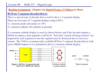
Seven-Segment Displays • Recall that a seven-segment display has LEDs named a through g (and possibly one or two LEDs for decimal points) that can be lit up to display characters.
Common-Cathode or Common-Anode? • Every seven-segment display is either: • Common-cathode: each LED has its own anode pin, and all LEDs share a single cathode pin. • Or common-anode: each LED has its own cathode pin, and they all share a single anode pin. • The Dragon12’s are common-cathode.
Current-Limiting Resistors • Recall that LEDs will burn out if you pass too much current through them. • Each LED should always be connected in series with its own current-limiting resistor, typically between 220 Ω and 470 Ω. • So if you wire a seven-segment display, you’ll need about eight of these current-limiting resistors: one for each segment and decimal point. (This is already done for us on the Dragon12 board.)
Banks of Seven-Segment Displays • Often we use banks of several seven-segment displays to show several digits. • Example: For a clock that displays hours, minutes, and seconds, we’d need six seven-segment displays. • The result: a lot of connections and a lot of current-limiting resistors (if you take the “brute-force” approach described below).
Two Approaches to Controlling a Bank of Seven-Segment Displays • Brute force approach • Simple, but eats up a lot of resources (such as I/O ports on the HCS12). • Multiplexing approach • Harder to understand, but much more efficient in its use of limited resources (such as I/O ports).
Approach #1: Brute Force • Connect a seven-segment display’s eight anode pins through current-limiting resistors to one of the HCS12 chip’s ports. • Also connect the display’s common cathode pin to ground. • Driving several displays in this way will use several of the I/O ports on our HCS12 chip.
Approach #2: Multiplexing • In the second approach, we use a single HCS12 port to drive the anode pins on all of the displays. • We also connect the common-cathode pins to another HCS12 port. This lets us turn a particular display on (by making the common-cathode pin LOW) or off (by setting the common cathode pin HIGH).
Approach #2: Multiplexing (Cont.) • We sequence quickly through the displays, turning each one on for an instant: • Send out the code for the first display’s digit. • Turn the first display on by setting its cathode LOW and setting all of the other cathodes HIGH. • Brief delay. • Send out the code for the second display’s digit. • Turn the second display on by setting its cathode LOW and setting all of the other cathodes HIGH. • Brief delay. • And so on for each of the other displays. • Repeat the entire sequence from Step 1.
Seven-Segment Displays on the Dragon12 Trainer • Our trainer board uses the multiplexing approach for its four seven-segment displays. • See Schematic Diagram 4 and pages 24-26 of Dragon12 manual.
Reminder: You Must Configure Ports as Inputs or Outputs • We’ve seen that the seven-segment displays’ anode pins are wired to Port B and their common cathode pins are wired to Port P. • So to use the seven-segment displays, we must first configure Ports B and P as outputs.
Downloading a Program from CodeWarrior to the HCS12 • When CodeWarrior downloads a program to the HCS12, it does using a widely used standard called the Motorola S19 file format. (http://en.wikipedia.org/wiki/S19_(file_format)) • In Lab #3 you briefly examined an S19 file for a program that you were downloading. One line (or “record”) of that file looked like this:S109200086038B0520FE9F • See next slide for analysis of this record.
Analyzing a Record from an S19 File • We can break the record into five pieces:S1 09 2000 86038B0520FE 9F Address: The starting address in memory where the following data bytes are to be located. Data: The data bytes being downloaded. In our case, this is the machine code for a simple program. Checksum: For error-checking. It’s Record type: Identifies this record as a data sequence record containing a two-byte address. Byte Count: Tells how many bytes follow in this record.
Checksums • A checksum byte is an extra byte appended to data that is being transmitted. Its purpose is to allow error checking by the receiver. (Similar to a parity bit.) • There are different ways to compute checksum bytes. They’re all effective, as long as the sender and the receiver are using the same method. See next two slides for the checksum method used in S19 files.
Method for Generating the Checksum in an S19 Record • The sender uses the following method to calculate the checksum byte: • Add the byte count, the address bytes, and the data bytes, discarding any carries. • Take the one’s-complement of the sum. • The result of Step 2 is the checksum byte for this record.
Method for Checking the Checksum in an S19 Record • The receiver uses the following method to check for errors: • Add the byte count, the address bytes, the data bytes, and the checksum byte, discarding any carries. • The result should equal $FF. If it does not equal $FF, an error has occurred during transmission.