Download
1 / 4
40 likes | 58 Views
A combinational logic circuit is said to be independent of time since it gives the results based on present input not past input. This research is concerned about the comparison between currently existing full subtractor IC and the subtractor which is built efficiently in the 125nm and observing the distortion and changes caused in the result of both full subtractor. The behaviour of the efficient full subtractor is designed using tanner eda tools which was useful and the currently existing full subtractor is designed using xilnx software and lastly the layout for this research is designed with the help of multisim. With help of this research many newly created circuits can designed much more smaller. G. Hemanth Kumar | K. Gopi | P. Gowtham | G. Naveen Balaji "Area Efficient Full Subtractor Based on Static 125nm CMOS Technology" Published in International Journal of Trend in Scientific Research and Development (ijtsrd), ISSN: 2456-6470, Volume-2 | Issue-6 , October 2018, URL: https://www.ijtsrd.com/papers/ijtsrd18860.pdf Paper URL: http://www.ijtsrd.com/engineering/electronics-and-communication-engineering/18860/area-efficient-full-subtractor-based-on-static-125nm-cmos-technology/g-hemanth-kumar<br>

E N D
International Journal of Trend in International Open Access Journal International Open Access Journal | www.ijtsrd.com International Journal of Trend in Scientific Research and Development (IJTSRD) Research and Development (IJTSRD) www.ijtsrd.com ISSN No: 2456 ISSN No: 2456 - 6470 | Volume - 2 | Issue – 6 | Sep 6 | Sep – Oct 2018 Area Efficient Full Subtractor Based Area Efficient Full Subtractor Based on Static CMOS Technology 125nm G. Hemanth Kumar Hemanth Kumar1, K. Gopi1, P. Gowtham1, G. Naveen Balaji B.E Student, 2Assistant Professor SNS College of Technology, Coimbatore, Tamil Nadu Naveen Balaji2 1B.E Department of ECE, SNS College Tamil Nadu, India ABSTRACT A combinational logic circuit is said to be independent of time since it gives the results based on present input not past input. This research is concerned about the comparison between currently existing full subtractor IC and the subtractor which is built efficiently in the 125nm and observing the distortion and changes caused in the result of both full subtractor. The behaviour of the efficient full subtractor is designed using tanner eda tools which was useful and the currently existing full subtractor is designed using xilnx software and lastly the layout for this research is designed with the help of multisim. With help of this research many newly created circuits can designed much more smaller. Keyword: Full Subtractor, cmos, static 125nm, tanner, multisim, Xilinx, half subtractor I. INTRODUCTION a logic gate is a physical device implementing a Boolean expression that is, it performs a logical design operation on one or more binary inputs and produces a single binary output. In digital circuit theory, combinational circuits which is also called as time independent logic is a type of digit is implemented by Boolean circuits in which the output is the pure function of the input. has reduced propagation delay and it has faster addition logic full subtractor is a combinational logical design performs subtraction of two binary bits, one is said to be minuend and other is subtrahend, bor previous adjacent lower is minuend bit. This circuit has three inputs and two outputs ‘a’, ‘b’ and ‘c’, denote the minuend, subtrahend, and previous borrow, respectively. Difference and Borrow represent the difference outputs borrow, respectively. Subtractor and adders are used in almost all integrated adders and subtractors are used for education purpose but in order check a ouput of the full subtractor a student has to connect multiple gates required gate are integrated into a single chip .It will be easy to analyze the circuit very fastly and accurately. The Full subtractor constructed in this research paper is constructed in 125nm static CMOS technology. II. EXISTING SYSTEM A full Subtractor is a logic circuit build with two half subtractor. A half subtractor combinational logic area in which it performs basic binary subtraction. A half subtractor is a two bit logical circuit .A half subtractor is made multiple gates which performs very basic operations according to the connections made in the CMOS (Complementary Metal Oxide Semiconductor).Full subtractor is also a two bit logical three inputs and two output where ‘a’, considered to be inputs of the full subtractor whereas ‘difference’ and ‘borrow’ are the outputs of the the logical circuit. Gates used in the full subtractor are ‘xor’ gate, ‘and’ gate, ‘not’ gate. Generally gate are the building of the the combinational circuits .Gates are built using several numbers of transistor. law which states every six months number of the transistors used in a particular integrated circuit will be increased due to the technology enhancemen XOR gate is a combinational logic ‘1’ output when the number of ‘1’ XOR gate implements an exclusive or, that is, a ‘1’ output results if one, and only one, o gate is ‘1’. If both inputs are ‘0’ gate is ‘1’. If both inputs are ‘0’ or both are ‘1’, a ‘0’ A combinational logic circuit is said to be independent of time since it gives the results based on present input not past input. This research is concerned about the comparison between currently are used in almost all integrated circuits. as for now adders and subtractors are used for education purpose but in order check a ouput of the full subtractor a student has to connect multiple gates . If all the required gate are integrated into a single chip .It will be easy to analyze the circuit very fastly and accurately. The Full subtractor constructed in this research paper is constructed in 125nm static CMOS btractor which is and observing the distortion and changes caused in the result of both full subtractor. The behaviour of the efficient full subtractor is designed using tanner eda tools which isting full subtractor is EXISTING SYSTEM: ull Subtractor is a logic circuit build with two half designed using xilnx software and lastly the layout for this research is designed with the help of multisim. With help of this research many newly created circuits is a logic design in the combinational logic area in which it performs basic binary subtraction. A half subtractor is a two bit logical circuit .A half subtractor is made up of multiple gates which performs very basic operations according to the connections made in the CMOS (Complementary Metal Oxide Semiconductor).Full subtractor is also a two bit logical circuit. It consist of three inputs and two output where ‘a’, ’b’ and ‘c’ are considered to be inputs of the full subtractor whereas ‘difference’ and ‘borrow’ are the outputs of the the static CMOS, 25nm, tanner, multisim, Xilinx, half subtractor physical device implementing a that is, it performs a logical operation on one or more binary inputs and In digital circuit theory, combinational circuits which is also called as time independent logic is a type of digital logic which Boolean circuits in which the tput is the pure function of the input. has reduced propagation delay and it has faster addition logic. A combinational logical design that performs subtraction of two binary bits, one is said to be minuend and other is subtrahend, borrow of the previous adjacent lower is minuend bit. This has three inputs and two outputs. The inputs the minuend, subtrahend, and Gates used in the full subtractor are ‘xor’ gate, ‘and’ gate, ‘not’ gate. Generally gate are the building blocks he the combinational circuits .Gates are built using transistor. We know that Moore’s law which states every six months number of the transistors used in a particular integrated circuit will be increased due to the technology enhancement. The XOR gate is a combinational logic gate that gives a ‘1’ output when the number of ‘1’ inputs is odd. An gate implements an exclusive or, that is, a ‘1’ output results if one, and only one, of the inputs to the The The outputs outputs, represent the difference and Subtractor and adders @ IJTSRD | Available Online @ www.ijtsrd.com www.ijtsrd.com | Volume – 2 | Issue – 6 | Sep-Oct 2018 Oct 2018 Page: 1371
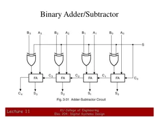
International Journal of Trend in Scientific Research and Development (IJTSRD) ISSN: 2456 International Journal of Trend in Scientific Research and Development (IJTSRD) ISSN: 2456 International Journal of Trend in Scientific Research and Development (IJTSRD) ISSN: 2456-6470 output results. In ‘and’ gate ,only multiplication operation can be done if the both input are same the output will be the same as the input and if the inputs are different then the output will ‘0’. In ‘not’ contains only one input and the output is the output of the input if the input is ‘1’ then the output will be ‘0’ vice versa. Fig-1.1: Block diagram of Half Subtractor: In ‘and’ gate ,only multiplication operation can be done if the both input are same the output will be the same as the input and if the inputs subtractor is a basic arithmetic processor which perform only subtraction its only function is to deduce a single bit binary from the input subtractor is a basic arithmetic processor which perform only subtraction its only function is to deduce a single bit binary from the input III. FULL SUBTRACTOR Half subtractor logical design has a major which we do not have the space to provide for the subtraction in half subtractor Subtractor logic, we can actually make a Borro input in the circuitry and could subtract it with other two inputs A and B. So, in the case of Circuit we have three inputs, A which is minuend, B which is subtrahend and Borrow In. On the other hand we get two f output, Difference and subtractor is basic combinatinal logic circuit which performs a single arithmetic function It consist of three input naming ‘a’, ‘b’, ‘c’ which takes the input and process the algorithm using multiple gates such as ‘xor’, ‘ Comparison between currently existing full subtract and newly area efficient full subtractor Fig2.1: Block diagram of Full Subtractor: Block diagram of Full Subtractor: . In ‘not’ gate, FULL SUBTRACTOR: logical design has a major flaw in which we do not have the space to provide input bit input and the output is the output of the input if the input is ‘1’ then the output will be ‘0’ ubtractor. In case of full , we can actually make a Borrow in input in the circuitry and could subtract it with other two inputs A and B. So, in the case of Full Subtractor we have three inputs, A which is minuend, B and Borrow In. On the other hand Difference and Borrow. A full subtractor is basic combinatinal logic circuit which performs a single arithmetic function i.e. subtraction. It consist of three input naming ‘a’, ‘b’, ‘c’ which takes the input and process the algorithm using multiple gates such as ‘xor’, ‘and’ and ‘not’. urrently existing full subtractor and newly area efficient full subtractor. Subtractor: Difference a Half Borrow Subtractor b In fig 1.1 we can analyze that a half subtractor consist of two inputs ‘a’ and ‘b’ and output ‘difference’ ‘borrow Fig-1.2: Logic diagram of Half Subtractor: U9 a b In fig 1.1 we can analyze that a half subtractor consist of two inputs ‘a’ and ‘b’ and output ‘difference’ and Logic diagram of Half Subtractor: Difference a Difference XOR2 Full U7 NOT b c Borrow Subtractor Subtractor U8 Borrow In fig 2.1 we can analyze that a full of two inputs ‘a’, ‘b’, and ‘c whereas ‘difference’ and ‘borrow AND2 at a full subtractor consist , and ‘c whereas output In fig 1.2 Gates like ‘xor’, ‘not’, and which are used to process the inputs and give the output. Each gate has a difference type of process algorithm based the connection given to the CMOS The Boolean expression of the half subtractor is as follows Difference = ab’ + ba’ Borrow = a. b Fig-1.3: Truth Table of Half Subtractor: a b Difference Borrow ‘not’, and ‘and’ Gates which are used to process the inputs and give the output. Each gate has a difference type of process connection given to the CMOS. The Boolean expression of the half subtractor is as Fig2.2: Logic Diagram of Logic Diagram of Full Subtractor: U1 U1 a bc Difference U6 NOT XOR3 XOR3 U2 Truth Table of Half Subtractor: AND2 U4 U3 Borrow Borrow 0 0 0 0 AND2 U5 OR3 1 1 1 0 AND2 1 1 0 0 When the inputs are given through the respective labels gates present the circuits will process the data and perform the arithmetic operation subtraction and produce the output difference and borrow difference and borrow 1 1 0 0 When the inputs are given through the respective labels gates present the circuits will process the data and perform the arithmetic operation subtraction and In fig 1.3 is a truth table of the half subtractor which portrays the output of that logical circuit. In fig 1.3 is a truth table of the half subtractor which circuit. A half @ IJTSRD | Available Online @ www.ijtsrd.com www.ijtsrd.com | Volume – 2 | Issue – 6 | Sep-Oct 2018 Oct 2018 Page: 1372
International Journal of Trend in Scientific Research and Development (IJTSRD) ISSN: 2456 International Journal of Trend in Scientific Research and Development (IJTSRD) ISSN: 2456 International Journal of Trend in Scientific Research and Development (IJTSRD) ISSN: 2456-6470 Fig2.3: CMOS Design of Full Subtractor: Full Subtractor: IV. B.1 OUTPUT: RESULTS: Waveform of Logic design of Waveform of Logic design of Full Subtractor: The above full subtractor is designed using static cmos algorithm under 125nm which is quite efficient and the results are same as the currently existing one Fig2.4: Truth Table of Full Subtra Truth Table of Full Subtractor: The above full subtractor is designed using static cmos algorithm under 125nm which is quite efficient and the results are same as the currently existing one Waveform of CMOS design of Waveform of CMOS design of Full Subtractor: a b c Difference Borrow Borrow 0 0 0 0 0 1 1 1 0 0 1 1 1 0 0 1 0 1 0 0 1 0 1 1 0 1 0 1 0 0 1 1 0 0 0 1 1 1 1 1 The above truth table is solved using the universal Boolean expression Difference=((a&(~b)&(~c) )| ((~a)&b&(~c))| ~b)&c)| (a&b&c)) The above truth table is solved using the universal CONCLUSION: It has been observed from the simulation results that performance of adder architectures varies with various CMOS design. The output of these two Full Subtractors are same. The current of Carry Look Ahead adder is 125nm.If the fabrication size reduced to less than 100nm, performance varies and can be (CMOS) technology. From this research t . From this research the (CMOS) ((~a)&b&(~c))| ((~a)&( (a&b&c)) It has been observed from the simulation results that ectures varies with various The output of these two designs of are same. The current fabrication size adder is 125nm.If the reduced to less than 100nm, the adder varies and can be absorbed using static Borrow = ( (~(a) & b ) | ( b & c) | ( c & (~a) )) Borrow = ( (~(a) & b ) | ( b & c) | ( c & (~a) )) The above table used to serve the universal expression of a logic gate function. A logic gate truth table shows each possible input combination to the gate or circuit with the final output depending upon the combination of these inputs. universal boolean A logic gate truth table shows each possible input combination to the output depending upon @ IJTSRD | Available Online @ www.ijtsrd.com www.ijtsrd.com | Volume – 2 | Issue – 6 | Sep-Oct 2018 Oct 2018 Page: 1373
International Journal of Trend in Scientific Research and Development (IJTSRD) ISSN: 2456 International Journal of Trend in Scientific Research and Development (IJTSRD) ISSN: 2456 International Journal of Trend in Scientific Research and Development (IJTSRD) ISSN: 2456-6470 7.E. M. M. Poncino, (1996) Static and Dynamic CMOS circuits, IEEE, International Conference on ASIC, 8.P. S. Aswale and S. Comparative Study of Different Low Power Design Techniques for reduction of Leakage power in CMOS VLSI Circuits, 8887,Volume 70-NO.1 9.R. L. Geiger, P. E. Allen, N. VLSI Design techniques for Analog and Digital Circuits, McGraw Hill, [page.No.597-ch7 10.S. Shobana, R. Ramya, K.K. Rashika, G. Naveen Balaji, K. Boopathiraja, “Hamming Window Function based FFT Analysis of Advanced Approximate Adder design in 125nm CMOS technology using International Journal of Science and Innovative Engineering & Technology, Vol. 5, Issue: May 2018. 11.G. NaveenBalaji, P. Malini, Shanmugavadivu, “14T Full Adder in 125nm CMOS technology for FFT applications using piecewise constant interpolation f(x) = 2.0”, Advances in Natural and Applied Sciences (Scopus), Vol. 12, Issue 9 (Sep 2018) pp: 17 ISSN:1995-0772 can be achieved by operating point within 0.9v. research is very useful and more advantageous in future microprocessor industries. REFERENCES 1.N. Weste and K. Eshraghian, --Principles of VLSI Design, A system perspective, Reading, Addison-Wesley, 1993. 2.Shital Baghel, Pranay Kumar Rahi, Yadav, 2015,”(CMOS) Half Adder Design & Simulation Using International al Journal of Innovative Science, Engineering & Technology(IJISET),Vol.2 Issue 3,pp.195-622,Aug.2000. 3.Ming-Bo Lin, “Introduction to VLSI systems A logic, circuit and system perspective,” Taylor & Fransis group, ch.7 4.Neil H. E. Weste, David Harris Ayan Banaerjee,”CMOS VLSI Design” Pearson Education, Inc., pp.11, Third edition, 2005. 5.M. Morris Mano, Michael D. Cilleti “Digital Design”,4th edition,pp.143,2012.. 6.Kaushik Roy and S. C. Prasad, CMOS VLSI circuit design”, 129,2000 point within 0.9v.This (1996) Power Consumption of CMOS circuits, IEEE, 2nd research is very useful and more advantageous in International Conference on ASIC, pp.425-427. S. Chopade, (2013) Comparative Study of Different Low Power Design Techniques for reduction of Leakage in CMOS VLSI Circuits, IJCA(0975- Principles of VLSI Reading, MA: Rahi, Nishant Allen, N. R. Strander (2013) Half Adder Design & VLSI Design techniques for Analog and Digital Circuits, McGraw Hill, New Delhi, India,. Simulation Using Different Different al of Innovative Science, Technology(IJISET),Vol.2 Issue Foundry”, Foundry”, S. Shobana, R. Ramya, K.K. Rashika, G. Naveen ji, K. Boopathiraja, “Hamming Window Function based FFT Analysis of Advanced Approximate Adder design in 125nm CMOS technology using International Journal of Science and Innovative Engineering & Technology, Vol. 5, Issue: May Bo Lin, “Introduction to VLSI systems A logic, circuit and system perspective,” Taylor & Transmission Transmission gates”, gates”, Harris Design”. Third edition, and Malini, T. Poovika, P. M. Morris Mano, Michael D. Cilleti “Digital gavadivu, “14T Full Adder in 125nm CMOS technology for FFT applications using piecewise constant interpolation f(x) = 2.0”, Advances in Natural and Applied Sciences (Scopus), Vol. 12, Issue 9 (Sep 2018) pp: 17-26, ”Low power Willey,pp.1- @ IJTSRD | Available Online @ www.ijtsrd.com www.ijtsrd.com | Volume – 2 | Issue – 6 | Sep-Oct 2018 Oct 2018 Page: 1374