Download
1 / 22
220 likes | 239 Views
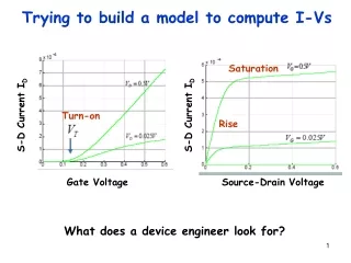
Device engineers aim to understand current saturation by building a toy model for effective computation of I-V characteristics. The study focuses on the conductance quantization in gold nanowires, broadening of energy levels, channel potential, and the impact of gate and drain voltages. By incorporating electrostatics and self-consistent fields, the model aims to provide insights into avoiding level slippage and achieving accurate current saturation in modern transistors.

E N D
Trying to build a model to compute I-Vs Saturation S-D Current ID S-D Current ID Turn-on Rise Gate Voltage Source-Drain Voltage What does a device engineer look for?
Toy Model : Current E E µ1 µ2 f1 f2 (weighted average of f1,2) (Only levels near EF conduct) (Net escape time 1/g = 1/g1 + 1/g2)
E E µ1 µ2 f1 Height 1/4kBT f2 Width kBT (-df0/dE)(m2-m1) (-df0/dE)qVD Finite temperature What does df0/dE look like?
E E µ1 µ2 f1 f2 1 - 0 MaximumConductance ?
E E µ1 µ2 f1 f2 MaximumConductance ? Conductance seems unlimited Experiment and calculation say otherwise !
G0 = 2q2/h = 77 mA/V Conductance quantization in gold nanowires EXPT Halbritter PRB ’04 Minimum resistance of a conductor (h/2q2 = 12.9 kW) Different from Ohm’s Law R = rL/A Modified Ohm’s Law R = r(L + L0)/A
Conductance quantization in gold nanowires EXPT Halbritter PRB ’04 G0 = 2q2/h = 77 mA/V Ohmic IV, quantized slope, fundamental constantsHow would this come from our equations?
E E µ1 µ2 f1 f2 For g1=g2, max conductance Solution: Broadening limits conductance “Spillage” Only fraction of level lies in m1-m2 window
Why do levels broaden? Fourier Transform P(t) D(E) t E Occupation probability Isolated channel Density of states (Sharp level) E=hn for quantum particles like electrons, photons Thus (t,E) form Fourier pairs
Why do levels broaden? e-t/t Fourier Transform e D(E) P(t) t E Occupation probability Channel coupled to contacts Density of states (Broadened level) D(E) = g/2p[(E-e)2 + (g/2)2] g = g1 + g2 = ħ/2t • Fourier transform of an exponent Lorentzian • peak value 2/pg, width ~ g • ∫D(E)dE = 1 (Sum rule Can still hold 1 electron)
µ1 µ2 M(E) Current with Broadening Landauer theory (“Conduction is Transmission”)
µ1 µ2 M(E) Current with Broadening Landauer theory (“Conduction is Transmission”)
Also need Voltage Drop across wire “Slippage” Why is that important?
z x Current saturation in FETs is compromised by ‘slippage’ E n-FET Gate µ2 µ1 Insulator CHANNEL W L D(E) Positive Drain bias attracts electrons towards it by lowering drain levels
But if gate sits too far to hold level fixed, level could slip down with applied drain bias! intel.com Current saturation in FETs is compromised by ‘slippage’ IV doesn’t saturate due to this ‘slippage’ E Drain current µ1 Modern day transistors µ2 D(E) Drain voltage Saturation once m2 crosses bandedge No more states to conduct from !
CGVG + CDVD VL = CS + CG + CD z x How would we avoid level slippage? Gate tries to hold levels, drain tries to move it For good gate control, VG must dominate VD in the Laplace potential E µ1 µ2 D(E) CG/CD (eox/esi)(L/tox) (1/3)(40) 13 for ‘good’ FETs Shrinking devices hurt L/tox But can’t shrink tox without oxide leakage Try to increase eox (ZrO2, HfO2, etc ‘high-k technology’) Gate Insulator CHANNEL W L
Thus potential is important to capture physics of slippage
How do we incorporate this potential? g1f1 + g2f2 N= dE D(E-U) g1 + g2 g1g2 g1 + g2 2q I1= dE D(E-U)[f1-f2] h Next: calculating U
A circuit model for the potential Q = -qDN = CSV + CG(V-VG) + CD(V-VD) CGVG + CDVD CGVG + CDVD qDN q2DN U = -q V = - + U0 CS + CG + CD CS + CG + CD UL CS + CG + CD CS + CG + CD d2V/dx2 = -qDN/e (Poisson equation)
Why DN and not simply N? U = qV = UL + U0(N-N0) The potential due to the background N0 electrons in a neutral channel is already included in the channel energy level e0 or its density of states Any extra charging term in U must therefore come only from charge imbalance (DN)!
µ2 Rate equation g1,2, f1,2 g1f1 + g2f2 g1f1 + g2f2 g1f1 + g2f2 + Broadening D(E) + Electrostatics U (Self-consistent Field) N= dE D(E-U) N= dE D(E ) N= g1 g2 g1 + g2 g1 + g2 g1 + g2 g1g2 g1g2 g1g2 µ1 g1 + g2 g1 + g2 g1 + g2 SOURCE DRAIN 2q 2q 2q I1= dE D(E)[f1-f2] I1= dE D(E-U)[f1-f2] I1= [f1-f2] CHANNEL h h h Poisson: U = UL + U0(N-N0) INSULATOR VG VD D(E) I Minimal Model for Transport Silicon / Nanotubes / Molecules (FetToy, CNTbands, MolCtoy)
g1f1 + g2f2 N= dE D(E-U) g1 + g2 g1g2 g1 + g2 SOURCE DRAIN 2q I1= dE D(E-U)[f1-f2] • Guess U • Nnew = aNold + (1-a)(Nnew – Nold) • Use converged U to find I CHANNEL h “Poisson”: N U Transport: U N U = UL + U0(N-N0) INSULATOR VG VD I Self-consistency