Thermoelectric Microgenerators with Nanometric Films
150 likes | 383 Views
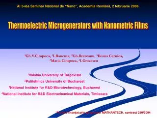
Al 5-lea Seminar N ational de “ Nano ”, Academia Rom ână, 2 februarie 2006. Thermoelectric Microgenerators with Nanometric Films. 1 Gh.V.Cimpoca, 1 I.Bancuta, 2 Gh.Brezeanu, 3 Ileana Cernica, 3 Maria Cimpoca, 4 I.Grozescu. 1 Valahia University of Targoviste

Thermoelectric Microgenerators with Nanometric Films
E N D
Presentation Transcript
Al 5-lea Seminar National de “Nano”, Academia Română, 2 februarie 2006 Thermoelectric Microgenerators with Nanometric Films 1Gh.V.Cimpoca, 1I.Bancuta, 2Gh.Brezeanu, 3Ileana Cernica, 3Maria Cimpoca, 4I.Grozescu 1Valahia University of Targoviste 2Politehnica University of Bucharest 3National Institute for R&D Microtechnology, Bucharest 4National Institute for R&D Electrochemical Materials, Timisoara Al Proiect finanţat prin programul MATNANTECH, contract 250/2004
INTRODUCTION A thermoelectric in-plane micro-generator with nanometric films has been fabricated using compatible standard semiconductor technologies (MEMS). The active material is a nanolayer polycrystalline silicon material laid on a dielectric membrane sustained by a silicon frame. Hicks and Dresselhouse predicted a huge increase of figure of merit ZT if the dimensionality of the electron system in thermoelectric materials is redused from 3D behaviour in bulk materials to 2D behaviour via nanoscaled layers. Reduced dimensionality offers one strategy for increasing ZT relative to bulk values [1-2]. The use of low-dimensional systems for thermoelectric applications is of interest because low dimensionality provides: (1) - a method for enhancing the density of states near EF, leading to an enhancement of the Seebeck coefficient; (2) - opportunities to take advantage of the anisotropic Fermi surfaces in multi-valley cubic semiconductors; (3) - opportunities to increase the boundary scattering of phonons at the barrier-well interfaces, without as large an increase in electron scattering at the interface, (4) - opportunities for increased carrier mobilities at a given carrier concentration when quantum confinement conditions are satisfied [3].
What makes a good Thermoelectric Material? • Figure of Merit ZT = (α2σ/K)T • T = Absolute Temperature • α2= (Seebeckcoefficient)2 • Tells how much average thermal energy is transported by each carrier • σ= electrical conductivity • Tells how much the carriers can transport energy without Joule loss • K = thermal conductivity • Tells how small is the reverse flow of heat from the cold-side to the hot-side, opposing the electron-transport of heat • Minimize thermal conductivity and maximize electrical conductivity • Has been the biggest dilemma for the last 40 years • Can the conflicting requirements be met by nano-scale material design? Efficiency versus ZT and DT
Big Jump in ZT with the Phonon-Blocking, Electron-Transmitting Structures With Advanced SemiconductorMaterials? • ZT need to improve over 1.3 at 300K for a major impact in electronics cooling and around 2.5 for a revolutionary impact in air – conditioning, and power from waste - heat
Some of Approaches • New Bulk Materials • Skutterudites (Rensselaer, Oak Ridge, JPL, 1992) • Cage – structures with ratting atoms to scatter phonons • Novel Chalcogenides and Clathrates (Michigan State and Arizona, 1994) • Complex Variations of Bi2Te3 to reduce phonon mean-free paths • Nano-scale Materials • Low-Dimensional Structures (MIT, Mit Lincon Labs, 1992) • Quantum – confinement to Enhance Density of states which increase Seebeck coefficient • Nano-scale Superlattice (RTI, 1992) • Phonon blocking from acoustic mismatch between superlattice components but electron-transmitting due to negligible electron-energy offsets • Heterostructure Thermionics (UCSB, Oak Ridge, 1996) • Thermionic-like effects using energy barriers that can be controlled in hetero-structures
Some Bulk Material and Nano-Material Progress • Cs Bi4Te6(Michigan State University) • Bulk Materials with a ZT~ 0.8 at 225K but less than 0.8 at 300K (Science 287, 1024-1027, 2000) • Filled Skuterrudites (JPL) • Bulk materials with a ZT ~1.35 at 900K(Proc. Of 15th International Conf. On Thermoelectrics, 1996) • PbTe/PbTeSe Quantum-dots (Harman, MIT Lincoln Labs.) • ZT~ 1.6 at 300K based on cooling data (Science 297, Sep. 2002) • Bi2Te3/Sb2Te3Superlattices(RTI) • ZT~2.4 at 300K in devices with all properties measured at the same place, same time, with current flowing and verified by two independent techniques (Nature, 597-602, Oct. 2001)
New Bulk Materials The skutterudite structure was originally attributed to a mineral from Skutterud (Norway) with a general formula (Fe, Co, Ni) As3. The skutterudite structure (cubic space group Im3, prototype CoAs3) is illustrated in figure. The unit cell contains 8 AB3 groups. The unit cell is relatively large and contains 32 atoms which indicates that a low lattice” thermal conductivity might be possible. For the state of the art thermoelectric materials such as PbTe and Bi2Te3 alloys, the number of isostructural compounds is limited and the possibilities to optimize their properties for maximum performance in different temperature ranges of operation are also very limited. The skutterudite unit cell of formula TPn3 (T- transition metal, Pn - pnicogen). Crystal type Chevrel
MICROGENERATORS WITH NANOMETRIC FILMS Experimental techniques and sample preparation
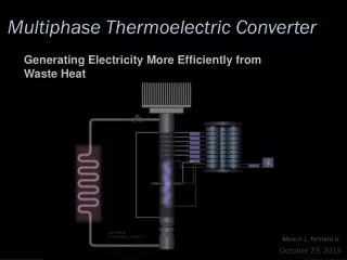
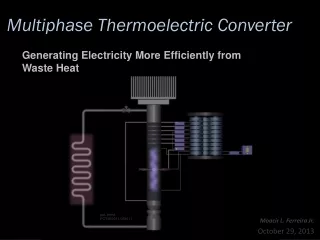
Modes Of Working Two modes of working are anticipated for the in-plane thermoelectric micro-generator. The first mode of working (i.e. mRTG) is when the heat source is on the membrane (Fig. 2a). The silicon frame that sustains the membrane is the cold side. A large temperature difference along the thermoelectric legs should be created with small heat sources because the thickness of the area covered by the thermoelectric leg is thin (1250 nm) and its thermal conductivity is low (3.9 W.m-1.K-1). This large temperature difference is interesting to get high efficiency. Fig.2b Fig.2a Fig.2b The second mode of working (i.e. BHPW) takes advantage of the large surface-to-volume ratio of the membrane to use it as a radiator, the hot side being the silicon frame (Fig. 2b). The heat source may be the heat generated by a living creature while the coolant could be simply air.
The fabrication method Low stress-silicon nitride and silicon dioxide sandwich layers were deposited on a <100>-oriented silicon wafer by low pressure chemical vapor deposition (LPCVD). A window was etched in the dielectric multilayer on the back of the silicon wafer by plasma etching. A polycrystalline silicon layer was deposited by LPCVD at 600°C and patterned by wet etching, to define the position of the thermoelectric legs on the front side of the wafer. Selected legs were implanted with boron (p-type) while other legs were implanted with phosphorus (n-type). Top view of a silicon-based thermoelectric micro-generator. Figure 2. Section of microgenerator
Experiment Using the model proposed by Koslov, assuming a onedimensionalheat transfer along the thermoelectric legs, anactive material with a low figure-of-merit and neglecting theheat losses by radiation and convection, it can be easilydemonstrated that the maximum electrical power producedby a mRTG, at a given heating power is obtained for athermoelectric leg thickness calculated from: K1 d1= K2d2 whereK1, K2 and d1, d2 are the thermal conductivities andthicknesses of the dielectric membrane and of thethermoelectric material, respectively The optimum leg length is calculated from: l2/l1=1/3 where l1 is half of the self-standing membrane width and l2 isthe thermoelectric leg length.
Advantages of Superlattice Thermoelectric Technology • Enhanced efficiency • Super-fast cooling and heating • Enhanced power density • Localized cooling/ heating technology • 1/40,000th the actual TE material requirement of bulk technology for same functionality – low recycle costs –Eco-friendly technology
CONCLUSION • A new family of promising thermoelectric materials with the skutterudite crystal structure has been presented. The possibilities of finding candidates for a particular operating temperature are great in such a large family of materials. Initial results obtained on some of their representatives demonstrate the great potential of skutterudites for high ZT values as very high mobility and very low lattice thermal conductivity can be obtained with materials of the same crystal structure. In particular, that if the high mobility of the binary skutterudite compounds can be somewhat preserved, there are several approaches for large reductions in thermal could lead to ZT values substantially larger than 1. • In-plane thermoelectric micro-generators are very promising for powering micro-systems. A heating power of about 100 mW may be enough to produce 1 mW of useful electrical power in vacuum, using thin film technology. • Thermoelectric micro-generators based on thick-film technology will be able to work in air. They will take advantage of their large surface-to-volume ratios to improve the coupling between the heat reservoirs and the thermo elements. This makes it a very promising device to efficiently convert heat wasted by our body to electrical power. A compact thermoelectric device may be able to produce as much as 60 mW with an output voltage of about 1.5 Volt. Nevertheless, the electrical contact resistances have to be lowered to a satisfactory level, good thermoelectric materials have to be used and thermoelectric thick-film technology needs to be improved or developed to get films with good thermoelectric properties at an acceptable economical cost.
REFERENCES [1] Hicks, L.D et al., “Effect of quantum-well structures on thermoelectronic figure of merit” Phys.Rev.B.Vol 47, No 19 (1993), pp.12727-12731 [2] Dresselhouse, M.S. et al., „Low Dimensional Thermoelectrics“, Proc.16 th International Conference on termoelectrics, Dresden, Germany, August 1997, pp 92-99 [3] D.-J. YAO, C.-J. KIM, and G. CHEN – „Design of thin-film thermoelectric microcoolers”, in HTD-Vol. 366-2, Proceedings of the ASME Heat Transfer Division – 2000, Volume 2, ASME 2000. [4] Gh.V.Cimpoca et all, „Physics and Modeling of Thermoelectric Microgenerators”, 6 th International Balkan Worckshop on Applied Physics, Constanta, Romania, 5-7 July, 2005.