Download
1 / 31
310 likes | 546 Views
CH712 물리화학특강 II 가을학기 강의 진도표 주제 : Nano Science and Technology ㅇ 강의담당 : 김세훈 , 유룡 , 김상율 , 김진백 , 이윤섭 , 이억균 , 곽주현 , 천진우 ㅇ 주관교수 : 김세훈 ㅇ 연락처 : 전화 : x2831; email:sehkim@kaist.ac.kr ㅇ 강의시간 : 화 , 목 16:00-17:30 ㅇ 강의실 : 자연과학동 2124 호

E N D
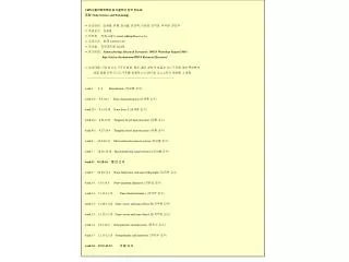
CH712 물리화학특강 II 가을학기 강의 진도표 주제: Nano Science and Technology ㅇ 강의담당: 김세훈, 유룡, 김상율, 김진백, 이윤섭, 이억균, 곽주현, 천진우 ㅇ 주관교수: 김세훈 ㅇ 연락처:전화: x2831; email:sehkim@kaist.ac.kr ㅇ 강의시간: 화,목 16:00-17:30 ㅇ 강의실: 자연과학동 2124호 ㅇ 참고문헌: Nanotechnology Research Directions: IWGN Workshop Report(1999) http://itri.loyola.edu/nano/IWGN.Research.Directions/ ㅇ 강의내용: 기능성 나노구조의 합성, 제조, 물리 화학적 성질과 나노구조에 대한 특성분석 방법 등을 다루고 나노구조를 응용한 나노센서 및 나노소자의 개념을 소개함. ------------------------------------------------------------------------------------------ week 1 : 9. 4 Introduction (김세훈 교수) week 1/2 : 9.6-9.11 Nano-characterization (김세훈 교수) week 2/3 : 9.13-9.18 Nano dvice I (김세훈 교수) week 3/4 : 9.21-9.25 Template based nanostructures (유룡 교수) week 4/5 : 9.27-10.4 Template based nanostructures (유룡 교수) week 6 : 10.9-10.11 Macromolecular nanostructures (김상율 교수) week 7 : 10.16-10.18 Macromolecular nanostructures (김상율 교수) week 8 : 10.20-26 중 간 고 사 week 9 : 10.30-11.1 Nano-fabrication and nano-lithography (김진백 교수) week 10 : 11.6-11.8 Nano-quantum chemistry (이윤섭 교수) week 11 : 11.13-11.15 Nano-thermodynamics (이억균 교수) week 12 : 11.20-11.22 Nano-sensor and nano-device II (곽주현 교수) week 13: 11.27-11.29 Nano-sensor and nano-device II (곽주현 교수) week 14: 12.4-12.6 Nanoparticles and nanowires (천진우 교수) week 15: 12.11-12.13 Nanoparticles and nanowires (천진우 교수) week 16 : 12.15-12.21 기 말 고 사
A Few10-9 Milestones 3.5 billion years ago The first living cells emerge. Cells house nanoscale biomachines that perform such tasks as manipulating genetic material and supplying energy. 400 B.C. Democritus coins the word "atom," which means "not cleavable" in ancient Greek. 1905 Albert Einstein publishes a paper that estimates the diameter of a sugar molecule as about one nanometer. 1931 Max Knoll and Ernst Ruska develop the electron microscope, which enables subnanometer imaging. 1959 Richard Feynman gives his famed talk "There's Plenty of Room at the Bottom," on the prospects for miniaturization. 1968 Alfred Y. Cho and John Arthur of Bell Laboratories and their colleagues invent molecular-beam epitaxy, a technique that can deposit single atomic layers on a surface. 1974 Norio Taniguchi conceives the word "nanotechnology" to signify machining with tolerances of less than a micron. 1981 Gerd Binnig and Heinrich Rohrer create the scanning tunneling microscope, which can image individual atoms. 1985 Robert F. Curl, Jr., Harold W. Kroto and Richard E. Smalley discover buckminsterfullerenes, also known as buckyballs, which measure about a nanometer in diameter. 1986 K. Eric Drexler publishes Engines of Creation, a futuristic book that popularizes nanotechnology. 1989Donald M. Eigler of IBM writes the letters of his company's name using individual xenon atoms. 1991 Sumio Iijima of NEC in Tsukuba, Japan, discovers carbon nanotubes. 1993 Warren Robinett of the University of North Carolina and R. Stanley Williams of the University of California at Los Angeles devise a virtual-reality system connected to a scanning tunneling microscope that lets the user see and touch atoms. 1998 Cees Dekker's group at the Delft University of Technology in the Netherlands creates a transistor from a carbon nanotube. 1999 James M. Tour, now at Rice University, and Mark A. Reed of Yale University demonstrate that single molecules can act as molecular switches. 2000 The Clinton administration announces the National Nanotechnology Initiative, which provides a big boost in funding and gives the field greater visibility. 2000 Eigler and other researchers devise a quantum mirage. Placing a magnetic atom at one focus of an elliptical ring of atoms creates a mirage of the same atom at another focus, a possible means of transmitting information without wires.
What is Nanotechnology ? • Creation ofuseful materials, device, and systemsthrough the control of matter on thenanometer scale • 2. Exploitation of novel properties and phenomena developed at that level http://itri.loyola.edu/nano/IWGN.Research.Directions/
Transistor vs Virus Functionswitch and amplifier self-reproduction Memory1 bit >>10,000 bit Production a few weeks < a day time
DRAM vs DNA DRAM DNA
Comparison: Microstructurevs. Nanostructure • Microstructure Nanostructure • Physics Semi-classical Quantum mechanical • Electron Particle –like Wave-like • nature • E or k-space Continuous Discrete • Current Continuous Quantized • Decision Deterministic Probabilistic • Fabrication Micro-fabrication Nano-fabrication • Surface area/ Small Very large • volume • Packing Low Very high
Current Scientific and Technological Advancements • Scaling laws and size-dependent properties of isolated nanostructures • - Taylor made materials by controlling the size and shape • Tools for characterization • - SPM, SEM, TEM, XM • Fabrication and synthesis • - nanocrystal,quantum dots by strained layer growth, nanotubes, • mesoporous inorganics, dendrimers etc • - e-beam lithography, X-ray lithography, Soft lithography • Computation • Emerging uses • - GMR head, nano systems for sequencing DNA, nano CD, RTD, SET, • new protective coatings, nanocatalysts, aerogels
Fundamental properties of isolated nanostructures • - size dependent properties, statistical fluctuations, the structure, • compositions, physico-chemical properties • Fundamental properties of ensemble of isolated nanostructures • - fundamental limits to the preparation of identical nanostructures • Assemblies of nanoscale building blocks • - coupling between nanostructure, chemical and mechanical • interactions, nanofabrication techniques, integration, assemblies • Evaluation of concepts for devices and systems • - interconnection, current flow, device isolation, fault-and defect • tolerant designs • Nanomanufacturing • Connecting nanoscience and biology • Molecular electronics Goals for Next 5-10 years
Scientific and Technical Infra structure • Tools for synthesis and fabrication, for characterization • Flexible research structure • Training the next generation of nanoscientists
Example : Natural Nanotechnology Dunin-Borowski et al, Science282, 1868 (1998) Magnetite(Fe3O4) nanoparticle size=25nm Each particle is as large as it can be and still remain a single magnetic domain Chains of nanocrystals used for navigation illustrate nature’s exploitation of a fundamental scaling to achieve maximum and most efficient use of magnetization.
Example:Biomolecular nanomachine Schematic diagram of the F1-ATPase biomolecular motor-powered nanomechanical device. (A) a Ni post (height 200 nm, diameter 80 nm) (B) the F1-ATPase biomolecular motor (C) a nanopropeller (length 750 to 1400 nm, diameter 150 nm) The device (D) was assembled using sequential additions of individual components and differential attachment chemistries
Example:Quantum Corral D. Eigler, IBM • Surface state electrons on Cu(111) were confined to closed • structures (corrals) defined by barriers built from Fe datoms. • A circular corral of radius 71.3 Angstrom was constructed in • this way out of 48 Fe adatoms.
Example: Self-assembled Quantum Dot Ge pyramid containing ~2000 Ge atoms on Si(100) Ge dome grown by PVD on a 600 C Si(100) R.S. Williams et al, Acc. Chem. Res. 32, 425 (1999)
. Example: Gold Nanocrystal R. Andres, Purdue Univ
Example: Carbon Nanotube • Ultimate fiber • Quantum wire • Nanocontainer C. Dekker
Example: Super Strong Materials Mechanical strenth: s ~ d-1/2 d: grain size
Not all nanotechnology lies 20 years hence, as the following sampling of already commercialized applications indicates. ?/td> Application:CatalystsCompany: ExxonmobilDescription: Zeolites, minerals with pore sizes of less than one nanometer, serve as more efficient catalysts to break down, or crack, large hydrocarbon molecules to form gasoline. ?/td> Application:Data storageCompany: IBMDescription: In the past few years, disk drives have added nanoscale layering-which exploits the giant magnetoresistive effect-to attain highly dense data storage. ?/td> Application:Drug deliveryCompany: Gilead SciencesDescription: Lipid spheres, called liposomes, which measure about 100 nanometers in diameter, encase an anticancer drug to treat the AIDS-related Kaposi's sarcoma. ?/td> Application:Manufacture of raw materialsCompany: Carbon NanotechnologiesDescription: Co-founded by buckyball discoverer Richard E. Smalley, the company has made carbon nanotubes more affordable by exploiting a new manufacturing process. ?/td> Application:Materials enhancementCompany: Nanophase TechnologiesDescription: Nanocrystalline particles are incorporated into other materials to produce tougher ceramics, transparent sunblocks to block infrared and ultraviolet radiation, and catalysts for environmental uses, among other applications. NANOPARTICLES are made by Nanophase Technologies. Applications: Nano for Sale
Application: Nanotube Transistor • S.J. Tans, A.R.M. Verschueren, and C. Dekker, Nature, 393, 49-52 (1998)
Applications:Artificial Photosynthesis Huynh et al (‘99), Gratzel et al(‘99)
Nanofabrication:Patterned magnetic Arrays Nanomagnet arrays fabricated using interferometric lithography combined with(a) electroplating, (b) evaporation, and (c) etching Topographic and magnetic images of the array of the electroplated Ni posts Light circle: spin up( “1”), dark circle: spin down (“0”) H.I. Smith et al, JAP 87, 5110 (2000), JAP 85,6160(1999)
Nanofabrication:Dip Pen Nanolithography S. Hong and C.A. Mirkin, Northwestern Univ.
Architectronic Magnetic Nanoparticles 2D Co-nanoparticle arrays for single particle per bit recording Nano spin valve structure Ferromagnetic Co-nanoparticles coated with nonmagnetic Cu layers Spin transistor Spin quantum computer Builing Blocks are Co-nanoparticles
Applications: Integrated Nanotechnology in Microsystems http://itri.loyola.edu/nano/IWGN.Research.Directions