Download
1 / 37
370 likes | 391 Views
Explore the world of ceramics, from structural to functional applications in modern technology. Learn about bonding principles, structures, imperfections, and innovative materials like Transparent Conductive Oxides (TCOs) and OLED technology. Discover the properties, applications, and advantages of ceramics and related materials.

E N D
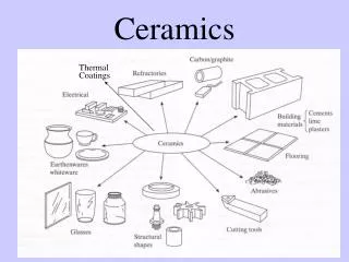
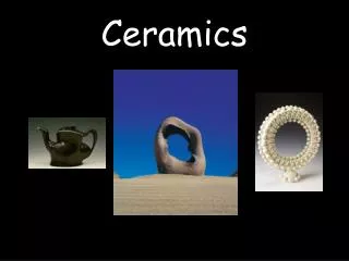
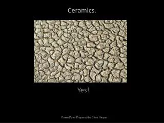
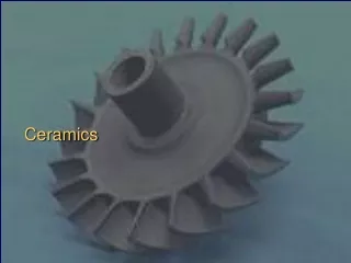
china/dishes cement/concrete functional ceramics structural ceramics electrons ionic – covalent bonding of at least 2 atoms (e.g. Al2O3: 63% ionic, SiC: 12% ionic) - anion + cation Ceramics inorganic – non-metallic materials structures depending on a) electrical charge b) atomic radii (rC/rA) stable – cations are in contact with surrounded anion
coordination number 4 rC/rA: coordination number 6 rC/rA: coordination number 8 rC/rA: Structure of Ceramics e.g.: Al2O3: Al3+: rC=0.053nm, O2-: rA=0.140nm
fcc anionic (Cl-) lattice fcc cationic (Na+) lattice AX Structures e.g. NaCl two interpenetrating fcc lattices: e.g. MgO, MnS, FeO (coordination number 6)
AmXp Structures e.g. CaF2 rC/rA=0.8 coord. 8 center cube positions only half-filled (CsCl completely-filled) AmBnXp Structures e.g. BaTiO3
octahedral interstitial positions Close Packing of Anions • e.g. ZnS • Zn anions in tetrahedral interstitial positions spinel structures, e.g. MgAl2O4: O2- fcc lattice, Mg2+ tetrahedral, Al3+ octrahedral
diffusion/electrical conduction Imperfections in Ceramics defects: electroneutrality: Schottky pair defect: cation and anion vacancy Frenkel pair defect: cation vacancy+interstitial non-stoichimetry: e.g. Fe1-xO, 2 Fe3+ ions – 1 Fe2+ vacancy, impurities
Transparent Conductive Oxides (TCOs) Wide band gap oxide semiconductors (ZnO, SnO2, In2O3 and mixed systems) High doping level (non-stoichiometry, substitution) Electron degeneracy, resulting in High electrical conductivity (n-type) High transmittance in the visible spectral range High infrared reflectivity
Applications of TCO thin films Solar cells & solar control: - Transparent front contacts for thin film photovoltaics Solar cells solar control
Displays - LCD (Liquid crystal display) - FPD (Flat panel display) - PDP (Plasma display panel) - Flexible display - PLED (Polymer light emitting device) - OLED (Organic light emitting device)
Flexible displays: Intrinsic shortcomings of LCDs: Viewing angle dependency, Low contrast and high power consumption Advantages of PLED: Excellent viewing angle, contrast and low power consumption Applications of flexible PLED: Electronic paper, smart cards, wearable devices Artist’s impression of the display of the future.
OLEDs Organic Light Emitting Device (OLED) technology is emerging as a leading next generation technology for electronic displays and lighting. OLEDs can provide desirable advantages over today’s liquid crystal displays (LCDs), as well as benefits to product designers and end users. OLEDs features: Vibrant colors High contrast Excellent grayscale Full-motion video Wide viewing angles from all directions A wide range of pixel sizes Low power consumption Low operating voltages Wide operating temperature range Long operating lifetime A thin and lightweight form factor Cost-effective manufacturability http://www.universaldisplay.com/tech.htm
Structure of OLEDs As this schematic shows, an OLED is a monolithic, solid-state device that typically consists of a series of organic thin films sandwiched between two thin-film conductive electrodes. The choice of organic materials and the layer structure determine the device’s performance features: emitted color, operating lifetime and power efficiency.
non-crystalline: SiO2 (addition of CaO, Na2O-network modifier – random networks) glass viskosity h [Pa s] temperature Silicate Ceramics O2- basic unit: SiO44- tetrahedron Si4+ crystalline: SiO2 (silica, high strength, relatively high Tm: 1710°C)
flexural strength/fracture strength: 3pt bending sfs=3FfL/2bd² F b x d d L Mechanical Properties of Ceramics/glasses brittle, no plastic deformation lower fracture strength than theoretical value -flaws (stress raisers) => statistical approach!!
Example: Investigated glass samples • Model-System • CaO / Al2O3 / SiO2 • Glass Sheets: • as received (10101 mm3) • Cross-section: • Crack induced by three-point-bending • All indents taken within 20min after cracking
Time dependent behavior under constant load: Strain Rate Sensitivity • Relaxation processes under constant load • strain rate sensitivity (m) describes this behavior:
Hardness and Moduli of the samples surfaces • Berkovich indenter / 10mN / 10s holding • significant influence of composition
Hydrated Silicates - Concrete Portland Cement Concrete: sand + gravel (about 60% packing) + cement Hydratation (simplified): 2(2CaO·SiO2)+4H2O=>3CaO ·SiO2 ·3H2O+Ca(OH)2 cement sand hydrates
Polymorphic Forms of Carbon diamond graphite • layers of hexagonally arranged C • covalent bond (3C) • between layers • weak van der Waals bond • good chemical stability/strength electric conductivity (electrodes/contacts) very strong bond (cubic diamond structure) each C bonds to 4 neighbours (ZnS structure) => hard, low electric/high thermal conductivity synthetic diamonds/thin films (tool surfaces)
CVD-Diamond deposition (M. Frenklach et al., 1991) Gas inlet Thermal or electric activation (HF, Flame, MWP, DC, ...) H2 + CH4 Hydrogen-dissociation Reactions in the gas-phase Kinetics, transport, surface-reactions, and carbon-incorporation Substrate (1) H2 = 2H (2) CH4 + H = CH3 + H2 (3) CH (s) + H = C (s) + H2 (4) C (s) + CH3 = C2H3 (s)
Microwave Plasma CVD TS = 500 – 1100°C, CH4/H2 = 0,5 - 2%, Pressure = 10 - 40 mbar P = 300 - 1500 W
Hetero-epitaxy of Diamond on Si SEM Jiang & Klages, Appl. Phys. Lett. 62, 3438 (1993)
Hetero-epitactic Diamond-films on Si(001) {111}-X-ray Pole-figure X. Jiang et al. J. Appl. Phys. 83, 2511 (1998) (001)Diamond // (001)Si [110] Diamond // [110] Si
Coating of cutting-tools Edge of a cutting-insert coated with (100)-diamond Micro-drill D = 0,15 mm used to machine circuit-boards
Adhesion issue limits potential applications Background: thermal stresses : thermal expansion coefficient of substrate and film : Young’s modul and Poisson-ratio of film Ts = 800 °C
Calculation of thermal stresses by FEM • Inherent good adhesion between Diamond-film and composite • Good adhesion of carbide-film on metallic substrate • Reduced maximum stress 1,2 GPa 1,94 GPa Diamant Diamond TiC/Diamond- Gradient layer TiC Steel Steel L. Xiang, PhD thesis TU-Braunschweig, 2002
SEM images of a Diamond/ß-SiC-composite-layer as well as its SIMS - depth profile
no composite-layer with composite-layer
Polymorphic Forms of Carbon fullerene C60 (discovered 1985) => carbon nanotube (C sheet + fullerene) hexagons and pentagons extremely strong (50-200GPa) stiff (1TPa) and ductile (fracture strain 5-20%) => ultimative fiber for composites, unique electric properties (metal/semiconductor)
Carbon nanostructures Single-wall-C-Nanotube (CNT) Multi-wall-CNTs: Van der Waals - bonding between individual layers, layer-spacing D=0,34 nm
Various single-wall CNTs • C-C bond-length: d=0.1421nm • Helical angels: θ= 0 – 30°
Production technologies • Arc-discharge (high quality, low productivity) • Laser-ablation (same as arc-discharge) • Chemical Vapor Deposition (CVD) Pyrolysis MPCVD HFCVD • Catalyst-based (Fe, Co, Ni, Pt, etc) growth • Orientated CNTs in combination with high productivity
Conductivity ranging from metallic to semi-conducting (helical angel, thickness) Low electric field strength for the onset of electron emission Ultra high axial mechanical stability: Young’s Modul = 5 TPa (single-wall-CNTs) Low radial mechanical stability Handling issues: grabbing, cutting, welding, and others Properties and potential applications • Nano-electronics • Scanning probes (AFM) • Electronfieldemission-Sources • Gas- and energy-storage • Biological micro-probes • Composite-material (polymers, concrete, and others) • Nano-cannula for bio- or medical-applications