Download

1 / 19
190 likes | 345 Views
FVTX Sensors and FPHX Chips FVTX Collaboration Meeting at UNM, 07/15/2009. Outline. Review Sensor Specifications Prototype Lot and Performance Production Order FPHX Prototype and Changes to 2 nd Round FPHX Production and Wafer Tests. 4 hermetic disks, z =18.5 to 38 cm.

E N D
FVTX Sensors and FPHX Chips FVTX Collaboration Meeting at UNM, 07/15/2009 Jon S. Kapustinsky
Outline • Review Sensor Specifications • Prototype Lot and Performance • Production Order • FPHX Prototype and Changes to 2nd Round • FPHX Production and Wafer Tests
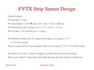
4 hermetic disks, z =18.5 to 38 cm FVTX Sensor Short Wedge Sensor HDI HDI Sensor FPHX chips (5 per column) Overall length 126.8 mm Overall width 8.8 mm i.r., 25.4 mm o.r. Overall length 50.1 mm Overall width 8.8 mm i.r., 15.3 o.r Jon S. Kapustinsky
A.5 Implant strips dimensions • 18 μm wide, p-implant strips, variable strip length on 7.5 degree opening angle, 2 columns of strips separated by a 75 μm gap between adjacent columns • Wedge A: strip length from 3.4 mm to 6.55 mm • Wedge B: strip length from 3.4 mm to 11.57 mm • A.6 Read-out strips • Aluminum, capacitively coupled over the p-implant with the processed aluminum edge, ≥ 1 μm along the entire strip length. • A.7 Bias Resistors • Overlap the implants or contained within the guard ring. • A.8 Sensitive region to cut-edge distance: 1.0 mm • A.9 Guard ring to cut edge distance: ≥ 300 μm • A.10 Guard ring design: Large contactable p-implant with overlapping aluminum. Contacts shall be in all four corners of the detector. • A.11 Read out pads: 150 x 50 μm wire bond pads, two staggered rows, one primarily for probing and one for bonding. • A.12 p-implant bias ring contacts at all four corners of the detector. • A.13 Spy pads to probe p-implants. • A.14 Back Contact: Contactable aluminum over highly doped n-implant. • A.15 Passivation: Sensors shall be passivated on front (microstrip) side. • A.16 Identification: Every 10th strip to be numbered, beginning at the bottom. Scratch pads for detector identification. Alignment marks for metrology. Jon S. Kapustinsky
Detector Electrical Specifications • C.1 Strips: p-implant. • C.2 Bulk dopant: n-type. • C.3 Readout strips: Aluminum ≤ 20 Ω/cm. • C.4 Bias resistors: 1.5 ± 0.5 MΩ polysilicon resistors. • C.5 Capactive coupling: ≥ 10 pF/cm. • C.6 Uniformity of resistivity: ± 25% wafer-to-wafer. • C.7 Depletion Voltage: < 100V. • C.8 Operation Voltage (Vop): Depletion Voltage + 50V. • C.9 Breakdown Voltage: Vop + 50V. • C.10 Leakage Current: ≤ 150 nA/cm2 at 20 degrees centigrade at Vop verified by vendor. • C.11 Current slope: at 20 degrees centigrade, I(Vop)/I(Vop – 50V) < 2. • C.12 Oxide breakdown voltage: > 50V (seller shall measure on a test device located on each wafer). • C.13 Detector current shall increase by no more than 25% after 12 hours of operation in dry air (RH ≤ 40%) at Vop (verified by LANL). Jon S. Kapustinsky
Bad Strips Shall Include But Not Be Limited To; • D.1 Capacitive coupling dielectric: short through dielectric at 50V. • D.2 Defective strips: Metal or implant opens, or shorts to neighbors. • D.3 Polysilicon resistors: Strip connection to resistor open. • D.4 Acceptance testing: Each aluminum strip shall be contacted with a probe and checked for shorts through the coupling dielectric at 50V by the seller. • D.5 Total strip acceptance: LANL requires a mean acceptance of 99% good strips in each delivery with no devices below 98%. • Seller Shall Supply Data Sheets for Each Detector As Follows; • E.1 IV curves: LANL requires the plot of I versus V up to 200V. • E.2 Depletion Voltage: LANL requires the value of the wafer depletion voltage. • E.3 Thickness: LANL requires the value for the wafer thickness. • E.4 Bad Strips: LANL requires the seller’s list of bad strips and the plot of capacitance versus strip number. Jon S. Kapustinsky
FVTX Sensors p-implant on n-bulk ac-coupled 1.5 MΩ polysilicon resistors Depletion voltage < 100V Resistivity 3 to 5 kΩ-cm P-Bias Ring Double Pad Rows P-Guard Ring N-Surround Polysilicon Resistors Initial Prototype, ON-Semi Current Prototype, Hamamatsu – shipped 31 October, 2008 Jon S. Kapustinsky
HPK Prototype Lot Jon S. Kapustinsky
I/V curves from prototype lot Beam test planned at pRad Facility at LANL with 800 MeV protons July-August Jon S. Kapustinsky
07/08/09 We understand your needs. We will make a drawing and send a proposal to you soon. We will put a strip number on Aluminum pattern on N-surround every 10ch strip. We will put a scratch pad, then show the serial number by BCD (binary-coded decimal). As for the lead time, it will be 4 months after receiving order but we will try to expedite the delivery of the sensors. Best Regards, Christine NishiyamaHamamatsu Sales Engineer Jon S. Kapustinsky
Basis for the production quantity for the FVTX sensors Required large wedge: (48x6) = 288 sensors Assume ~15% spares: 42 sensors Required with spares: 330 sensors (Management Plan 350?) Required small wedge: (48x2) = 96 sensors Assume ~15% spares: 15 sensors (historical discussions among FVTX’ers thought this too few, so increased to 24 spares) Required with spares: 120 sensors Jon S. Kapustinsky
FPHX readout chip FNAL ASIC Group Hoff, Yarema, Zimmerman Front End Core Slow Controller Vref + Shaper _ Comp Input Integrator Vth0 Comp FIFO/Serializer Vth1 Phase Block Comp Vth7 T-peak ~ 60 ns (programmable) Chip size 2.7 x 9.1 mm Program gain and Vref 128 channel 50, 66, 100, 200 mV/fC 60 ns peak time (rt- pgmbl) 3—bit ADC (th-pgmbl) Optimized to 1 to 2.5 pf input 115e + 134e/pf ~ 70 to 140 uW/ch (dep. gain) Fully functional chip design submitted through MOSIS TSMC 0.25 micron process (delivered Aug. 08) Programmable Thresholds Jon S. Kapustinsky
FPHX Chip back-end organization Data Processing 20 bits Analog Data Output Phase Control Data push architecture 10 MHz beam clock (BCO) 200 MHz data clock Zero suppressed Output 4 hits/chip in one BCO Approx. 300 uW/ch Serial Interface R/W Jon S. Kapustinsky
Variety of test bench results from LANL, Nevis and UNM indicate repeatable performance Threshold turn-on curve Jon S. Kapustinsky Shaper output from pulse inject ADC linearity
FPHX Changes for 2nd MOSIS Prototype submitted June 3, 2009 • Due 1st week of August • Threshold dispersion • Increase channel gain settings: 46,50,60,67,85,100,150,200,mV/fC • W/L input transistor selection optimized • Enable R/O on either serial output line, serialout1 or serialout2 or both • Add 7th time stamp bit (drop last word bit - we don't use it) • Fix the logic bug that Jim found that results in a mis-id of time-stamped events under certain timing conditions • New FPHX Chip Documentation sent on June 4, 2009 and it is posted on the FVTX Twiki (FPHX2_June2009Revision.doc) Jon S. Kapustinsky
Changes to the serial output word Original Serial Output Word Current Serial Output Word Jon S. Kapustinsky
MOSIS Production Order Quotation Jon S. Kapustinsky
Basis for the production quantity for the FPHX Chips Required: (26x48x6) + (10x48x2) = 8,448 chips installed Assume 10% spares: 845 chips Required with spares: ~9300 chips Chip/wafer estimate from Ray (2007): 1088 chips/wafer (approximately 85% reticle-to-wafer area) Initial minimum production: order 6 guaranteed(12 wafers started, typically 10 wafers completed), 6,528 - 10,880 chips (>85% yield on 10 wafers to meet requirement) Alternate production: order 12 guaranteed (24 wafers started, typically 20 or more completed) 13,056 – 21,760 Jon S. Kapustinsky
FNAL wafer probe testing FPHX Meeting at FNAL 7/21/2009 “cost benefit” of probe complexity Jon S. Kapustinsky