Download
1 / 33
330 likes | 576 Views
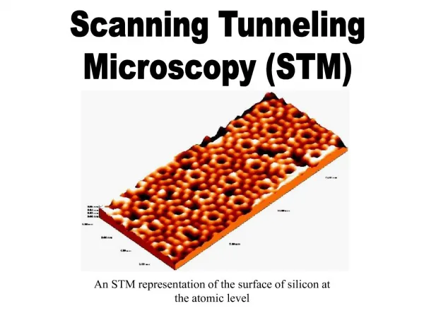
Scanning Tunneling Microscopy. By Lucas Carlson Reed College March 2004. Image from an STM. Iron atoms on the surface of Cu(111). The Scanning Tunneling Microscope (STM). The STM is an electron microscope that uses a single atom tip to attain atomic resolution. History.

E N D
Scanning Tunneling Microscopy By Lucas Carlson Reed College March 2004
Image from an STM Iron atoms on the surface of Cu(111)
The Scanning Tunneling Microscope (STM) The STM is an electron microscope that uses a single atom tip to attain atomic resolution.
History The scanning tunneling microscope was developed at IBM Zürich in 1981 by Gerd Binning and Heinrich Rohrer who shared the Nobel Prize for physics in 1986 because of the microscope. Gerd Binning Heinrich Rohrer
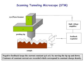
General Overview An extremely fine conducting probe is held about an atom’s diameter from the sample. Electrons tunnel between the surface and the tip, producing an electrical signal. While it slowly scans across the surface, the tip is raised and lowered in order to keep the signal constant and maintain the distance. This enables it to follow even the smallest details of the surface it is scanning.
The Tip 150x Magnification As we will see later, is very important that the tip of the probe be a single atom. Tungsten is commonly used because you can use Electro-chemical etching techniques to create very sharp tips like the one above.
Quantum Tunneling Classical Wave Function For Finite Square Well Potential Where E<V Classically, when an object hits a potential that it doesn’t have enough energy to pass, it will never go though that potential wall, it always bounces back. In English, if you throw a ball at a wall, it will bounce back at you.
Quantum Tunneling Quantum Wave Function For Finite Square Well Potential Where E<V In quantum mechanics when a particle hits a potential that it doesn’t have enough energy to pass, when inside the square well, the wave function dies off exponentially. If the well is short enough, there will be a noticeable probability of finding the particle on the other side.
Quantum Tunneling The finite square well potential is a good approximation for looking at electrons on conducting slabs with a gap between them.
Quantum Tunneling More graphs of tunneling: n(r) is the probability of finding an electron V(r) is the potential An electron tunneling from atom to atom:
Quantum Tunneling Now looking more in depth at the case of tunneling from one metal to another. EF represents the Fermi energy. Creating a voltage drop between the two metals allows current. Sample Tip
Quantum Tunneling Through a barrier, quantum mechanics predicts that the wave function dies off exponentially: So the probability of finding an electron after a barrier of width d is: And: Where f(V) is the Fermi function, which contains a weighted joint local density of states. This a material property obtained by measurements.
Quantum Tunneling Where: Plugging in typical values for m, d, and phi (where phi is the average work function of the tip and the sample), when d changes by 1 Å, the current changes by a factor of about 10!
Quantum Tunneling So if you bring the tip close enough to the surface, you can create a tunneling current, even though there is a break in the circuit. The size of the gap in practice is on the order of a couple of Angstroms (10-10 m)! As you can see, the current is VERY sensitive to the gap distance.
Quantum Tunneling The second tip shown above is recessed by about two atoms and thus carries about a million times less current. That is why we want such a fine tip. If we can get a single atom at the tip, the vast majority of the current will run through it and thus give us atomic resolution.
Note A STM does not measure nuclear position directly. Rather it measures the electron density clouds on the surface of the sample. In some cases, the electron clouds represent the atom locations pretty well, but not always.
Small Movements To get the distance between the tip and the sample down to a couple of Angstroms where the tunneling current is at a measurable level, STMs use feedback servo loops and converse piezoelectricity.
Servos Servos are small devices with a shaft that can be precisely controlled with electrical signals. Servos are used all the time in radio controlled cars, puppets, and robots.
Converse Piezoelectricity Piezoelectricity is the ability of certain crystals to produce a voltage when subjected to mechanical stress. When you apply an electric field to a piezoelectric crystal, the crystal distorts. This is known as converse piezoelectricity. The distortions of a piezo is usually on the order of micrometers, which is in the scale needed to keep the tip of the STM a couple Angstroms from the surface. Electric Field Pizos The tip
Problems and Solutions • Bringing the tip close to the surface and scanning the surface • Feedback Servo Loops • Keeping the tip close to the surface • Converse Piezoelectricity • Creating a very fine tip • Electro-chemical etching • Forces between tip and sample • Negligible in most cases • Mechanical vibrations and acoustic noise • Soft suspension of the microscope within an ultra high vacuum chamber (10-11 Torr) • Thermal length fluctuations of the sample and especially the tip • Very low temperatures • The sample has to be able to conduct electricity • There is no way around this, try using an AFM
Vibration-Isolation The original STM design had the tunnel unit with permanent magnets levitated on a superconducting lead bowl. They used 20 L of liquid helium per hour.
Vibration-Isolation The simple and presently widely used vibration protection with a stack of metal plates separated by viton - an ultra high vacuum compatible rubber spacer.
Original Trace Si(111) trace taken in 1983.
Processed Trace Computer processed version of the same trace of Si(111)
How to Process a Trace The trace (1) can be interpreted as a grid which can be shown as a grayscale picture (2). 2 3 1 4 The grayscale picture can be interpreted as a contour map (3) which can then be averaged out to make smooth (4) and finally colored (below).
Uses of STM Measuring high precision optical components and disk drive surface roughness of machined or ground surfaces is a common use for STM. Below is a trace of an individual turn mark on a diamond-turned aluminum substrate to be used for subsequent magnetic film deposition for a high capacity hard disc drive. 1 micron
Uses of STM By measuring variations in current, voltage, tip/surface separation, and their derivatives, the electronic properties of different materials can be studied. One such element studied was the bucky ball (C60). When you press down on a bucky ball by 1/10th nm, it lowers the resistance of the bucky ball by 100 times. C. Joachim J. K. Gimzewski, "An electromechanical amplifier using a single molecule”, Chemical Physics Letters, Vol. 265, Nos. 3-5, page 353, February 7, 1997.
Different STM Ideas You could decide not to use piezoelectricity to keep the distance between the tip and the surface equal at all times, and instead use the current measurements to determine the surface of a sample. Pros: • You can scan much faster Cons: • The surface must not have cavities more than a few Angstroms deep (an atom or two) because of tunneling
Different STM Ideas Imagine increasing the tunneling current when you are on top of an atom by lowering the tip a little. The attractive force between the tip and the atom would then increase, allowing you to “drag” atoms around. IBM imagined this. Iron atoms were first physisorbed (stuck together using intermolecular forces, aka Van Der Waals foces) on a Cu surface. The iron atoms show up as bumps below.
Different STM Ideas The iron atoms were then dragged along the surface of to form a circle.
Different STM Ideas Iron atoms on the surface of Cu(111)
References Carbon Monoxide Man G. Binnig and H. Rohrer. "Scanning Tunneling Microscopy", IBM J Res. Develop., 30:355, 1986. G. Binnig, H. Rohrer, “Scanning Tunneling Microscopy - From Birth to Adolescence”, Nobel lecture, December 8, 1986. Tit-Wah Hui, “Scanning Tunneling Microscopy - A Tutorial”, http://www.chembio.uoguelph.ca/educmat/chm729/STMpage/stmtutor.htm Wikipedia, “Scanning Tunneling Microscope”, http://en.wikipedia.org/wiki/Scanning_tunneling_microscope Nobel e-Museum, “The Scanning Tunneling Microscope”, http://www.nobel.se/physics/educational/microscopes/scanning/index.html Pictures from http://www.almaden.ibm.com/vis/stm/blue.html Carbon Monoxide on Platinum (111)