Download
1 / 45
450 likes | 469 Views
This project defense outlines the verification process of design revisions in NAND Flash memory, focusing on physics behind Flash Cell, Tunneling, Threshold Voltage Modulation, and more. It emphasizes Transaction Level Modeling for efficient functional verification.

E N D
Master’s Defense Chaitanya Bandi Dept. of ECE, Auburn University Fully configurable hierarchical transaction level verifier for functional verification Project Advisor: Dr.Vishwani D. Agrawal Committee Members: Dr.Victor P. Nelson, Dr. Fa F. Dai Dept. of ECE, Auburn University Chaitanya: MEE Project Defense
Outline • Problem Statement • NAND Flash Memory Design • Regression Testing • Transaction Level Verification • Microcode Regression • Comparison at a glance • Controllable comparison • Results and Future Work Chaitanya: MEE Project Defense
Problem Statement To verify the functional correctness of design revisions of the fullchip netlists in NAND Flash memory design group, Intel Corporation, Folsom, CA. Chaitanya: MEE Project Defense
Physics behind Flash Cell Chaitanya: MEE Project Defense
Flash Transistor Structure FG CG Chaitanya: MEE Project Defense
Threshold Voltage Modulation • The threshold voltage, Vthof a transistor is the gate voltage required to invert the channel and allow the conduction of electrons from the source to drain. • Information is stored in and erased from the flash cell by adding or removing electrons from the floating gate. • The voltage Vth can be modulated by adding or removing electrons from the floating gate. Chaitanya: MEE Project Defense
Erased Cell Vs Programmed Cell a) Erased cell b) Programmed cell A flash cell can exist in one of the two states, erased or programmed. Chaitanya: MEE Project Defense
Reading from a erased cell a) Erased cell b) Erased cell after application of gate voltage An application of Vg = 0-0.8Vresults in a current flow from the source to the drain which is represented as a logic ‘1’ in the cell. Chaitanya: MEE Project Defense
Reading from a programmed cell a) Programmed cell b) Programmed cell after application of gate voltage • An application of Vg = 0-0.8V does not result in a current flow from the source to the drain which is represented as a logic ‘0’ in the cell. • The threshold voltage required in this case is greater than the actual Vth of the device because of the presence of electrons on the floating gate. • This change in the required threshold voltage is due to the principle of Threshold Voltage modulation. Chaitanya: MEE Project Defense
Tunneling • Tunneling is referred to as the phenomenon where electrons can tunnel through an oxide layer. • This is achieved in the presence of a huge potential difference applied across the oxide. Chaitanya: MEE Project Defense
Programming a flash cell a) Erased cell b) Programmed Cell Electrons in the substrate move through the gate oxide and are trapped in the floating gate by the phenomenon of Tunneling. Chaitanya: MEE Project Defense
Erasing a flash cell a) Programmed cell b) Erased cell Electrons that are trapped in the floating gate move through the gate oxide into the substrate through the phenomenon of Tunneling. Chaitanya: MEE Project Defense
Why NAND Flash • NAND Flash Array Architecture makes its cell size almost half compared to a NOR cell. Chaitanya: MEE Project Defense
Intel’s new 34nm 32Gb NAND Flash chip Courtesy: http://www.intel.com/pressroom/archive/releases/20080529comp.htm
Regression Testing • Testing a program after it has been modified. • Major component in the program maintenance phase. • Checks the correctness of the new logic, • Ensures the continuous working of the unmodified portions of a program, • Validates that the modified program as a whole functions correctly. Chaitanya: MEE Project Defense
How is Regression Testing done? Stimulus Test Model Golden Model Response Response Comparison Chaitanya: MEE Project Defense
Abstraction Levels Abstraction TLM System Level RTL Transaction Level TLM RTL RTL Gate Level Transaction Level Transistor RTL Gates Transistors Layout Chaitanya: MEE Project Defense
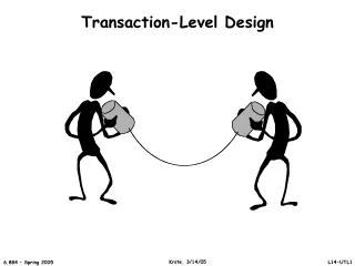
Transaction Level Modeling • RTL is too low level of abstraction for system level design. • Reducing and encapsulating details of design into transactions allows the designer to get a quick perception of the whole design in terms of its functionality. Chaitanya: MEE Project Defense
TLM Vs RTL • Details of communication among modules • Communication is done using Transactions • Details of implementation of modules • Implementation is at the signal level Chaitanya: MEE Project Defense
Example • A transaction level model would represent a read or write protocol using a single function call, with an object representing the request and another object representing the response. • An RTL HDL model would represent such a read or write protocol as a series of signal assignments and signal read operations. Chaitanya: MEE Project Defense
Benefits of TLM • Embedded Software Development • Functional Verification Chaitanya: MEE Project Defense
Embedded Software Development • Hardware models upon which embedded software is to be tested are available earlier in the design cycle in the form of transactions. • Software development usually starts only after the hardware prototype is available. HW SW Co-design and Validation Chaitanya: MEE Project Defense
Functional Verification • TLM models help the verification engineers to • Develop targeted tests that help in system verification as a whole. • Design hierarchical verification methodologies. Chaitanya: MEE Project Defense
Functional Verification in systems with RTL-only design • Functional verification can still be done using hierarchical verification methodologies. • The verification environment must have an ability to extract transactions. Chaitanya: MEE Project Defense
How are transactions extracted? • NAND Flash Memory Chip contains a microcode processing unit, the controller. • Instructions or microcode being executed in a simulation by the controller are modeled as transactions. Chaitanya: MEE Project Defense
The Controller • When the controller receives a “read” or a “write” instruction, it sends out signals on the bus to receive the data in the memory or to write to the memory respectively. • During a simulation, these series of instructions are tracked as microcode instructions and modeled as transactions for the purpose of functional verification. Chaitanya: MEE Project Defense
Verification Environment • Verification environment currently in NAND Flash design group involves • A Step-by-step review of microcode in execution using the fullchip simulation information. • Waveform comparison of the golden and test simulation results. Chaitanya: MEE Project Defense
Verification Environment Verifies the algorithm flow Manual review of microcode in execution Microcode Flow Verifies the signal flow Waveform Comparison Signals Chaitanya: MEE Project Defense
Drawbacks a) Review of the microcode in execution • Extremely manual • Excessive domain knowledge • Prone to human errors Chaitanya: MEE Project Defense
Drawbacks b) Waveform comparison of golden and test simulation data results in • irrelevant differences • comparing huge waveform databases which is very time-consuming Chaitanya: MEE Project Defense
Proposed Solution • A verification environment in which • Algorithm flow is checked automatically. • Controllable comparison of waveform database. • Algorithm details at the transaction level and signal details at the RTL are verified simultaneously. Chaitanya: MEE Project Defense
Hierarchical Transaction Level Verifier Chaitanya: MEE Project Defense
Features of the Verifier • Model system functionality as transaction packets. • Each packet can further contain sub transactions. • This forms a hierarchical model. • The leaf in the hierarchical verifier is at the signal level. Chaitanya: MEE Project Defense
Controllable Comparison • User can configure whether to step into a transaction packet or not based on its relevance in the hierarchy tree. • The signals that are to be compared can also be configured based on their relevance to the parent packet. Chaitanya: MEE Project Defense
Microcode Regression • A set of stimulus is applied to the golden netlist and the test netlist. • Response is recorded as both microcode flow from the data in the log files and signal flow is determined from the waveform database. Chaitanya: MEE Project Defense
Microcode Comparison Algorithm • Let the microcode flow in the golden and test cases can be modeled as MG and MT, where MG = { mG1,mG2,...,mGi,..mGn} and MT = { mT1,mT2,...,mTi,..mTn}. Chaitanya: MEE Project Defense
Microcode Comparison Algorithm • Compare the microcode instruction of Golden and Test cases mGi and mTi • If mGi and mTi matches, store the time slices between which these instructions take place. Mark it as a good time slice. • If mGi and mTi don’t match, store the time slices between which these instructions take place. Mark it as a bad time slice. • Perform an event based signal comparison only during the time slices at which there is a microcode match. Chaitanya: MEE Project Defense
Algorithm in execution Chaitanya: MEE Project Defense
Slicing based signal comparison Chaitanya: MEE Project Defense
Microcode Comparison Algorithm Chaitanya: MEE Project Defense
Controllable comparison Golden Test If the microcode flow matches, then only Compare the events on the signals during this transaction. (Waveform compare) Match? Don't compare Chaitanya: MEE Project Defense
Automation • “Slice” the golden simulation into Microcode Execution Slices. • Determine how signals change for each Microcode Execution Slice. • Store the information • Read the Test waveform and perform similar slicing. • Compare signal changes (or signal status) for each Microcode Execution Slice that has been validated. • Process, and report differences. Chaitanya: MEE Project Defense
Results • Simulation is perfomed in Cadence NCVerilog simulator. • Microcode comparison is done using the Transaction-Level verifier in PERL scripting language. • Signals are compared using the EventCom, a waveform comparison tool that uses SimVisionTM database. Chaitanya: MEE Project Defense
Conclusion • The entire process is automated and hence the turnaround time for validating each netlist revision is reduced from several days to several hours. • In the event of a mismatch in the simulation results, the verification engineer can identify which portions of the microcode flow is not being validated and take measures appropriately. Chaitanya: MEE Project Defense
Future Work • In future, we can have additional features to have the capability of viewing the transactions in the waveforms. • This will enable the verification engineers to graphically visualize the transactions and signals simultaneously in the waveform window. Chaitanya: MEE Project Defense