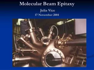
Molecular Beam Epitaxy
1.08k likes | 2.26k Views
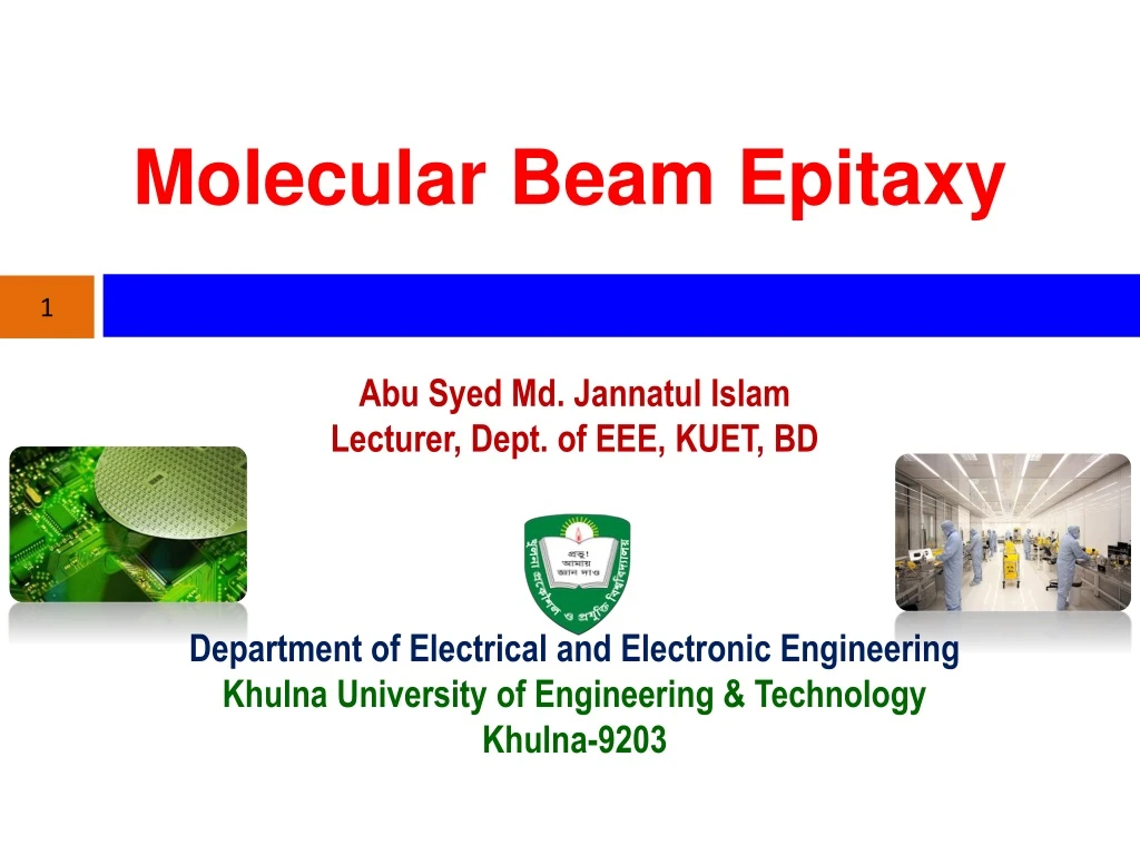
Molecular Beam Epitaxy. 1. Abu Syed Md. Jannatul Islam Lecturer, Dept. of EEE, KUET, BD. Department of Electrical and Electronic Engineering Khulna University of Engineering & Technology Khulna-9203. Molecular Beam Epitaxy (MBE ). 2.

Molecular Beam Epitaxy
E N D
Presentation Transcript
Molecular Beam Epitaxy 1 • Abu Syed Md. JannatulIslam • Lecturer, Dept. of EEE, KUET, BD • Department of Electrical and Electronic Engineering • Khulna University of Engineering & Technology • Khulna-9203
Molecular Beam Epitaxy(MBE) 2 • Molecular-beam epitaxy (MBE) process was developed in the late 1960s at Bell Telephone Laboratories by J. R. Arthur and Alfred Y. Cho. • Growth of epitaxial films on a hot substrate from molecular beams under ultra-high vaccum conditions(10−8–10−12Torr). • For III-V semiconductors (also used for IV, II-Vis, metals, oxides etc.) • The absence of carrier gases, as well as the ultra-high vacuum environment, result in the highest achievable purity of the grown films.
Molecular Beam Epitaxy(MBE) 3 • MBE is widely used in the manufacture of semiconductor devices, including transistors, and it is considered one of the fundamental tools for the development of nanotechnologies • It is also used for the deposition of some types of organic semiconductors. In this case, molecules, rather than atoms, are evaporated and deposited onto the wafer. • MBE systems can also be modified accordingly to the needs. Oxygen sources, for examples, can be incorporated for depositing oxide materials for advanced electronic, magnetic and optical applications, as well as for fundamental research.
Molecular Beam Epitaxy(MBE) 6 • Here in MBE reactants are introduced by molecular beams. • Create beams by heating source of material to melting point in an effusion (or Knudsen) cell. • Both solid and gas source can be used. • Pyro-lytic boron nitride (PBN) is chosen for crucibles which is chemically stable up to 1400’C). • Molybdenum and Tantalum are widely used for shutters. • Ultrapure materials are used as source. • The solid source (sublimation) provides an angular distribution of atoms or molecules in a beam. • The gaseous elements can crack/condense on the wafer where they may react with each other • Several sources (several beams of different materials) aimed at substrate
Molecular Beam Epitaxy(MBE) 7 • UHV gives source molecules a large mean free path, forming a straight beam. • Beam impinges on a heated substrate (600’C). • The beams can be shuttered in a fraction of second. A computer controls shutters in front of each furnace, allowing precise control of the thickness of each layer, down to a single layer of atoms. Intricate structures of layers of different materials may be fabricated this way. Such control has allowed the development of structures where the electrons can be confined in space, giving quantum wells or even quantum dots. • Incident molecules diffuse around the surface to the proper crystal sites and form crystalline layers.
Molecular Beam Epitaxy(MBE) 8 • Atoms on a clean surface are free to move until finding correct position in the crystal lattice to bond • Characterization tools allow growth to be monitored in-situ. • During operation, Reflection High-Energy Electron Diffraction (RHEED) is often used for monitoring the growth of the crystal layers. • Mass spectrometer for monitoring the residual gases and checking source beams for leaking. • A cryogenic screening around the substrate as a pump for residual gases. • Such layers are now a critical part of many modern semiconductor devices, including semiconductor lasers and light-emitting diodes. • The term "beam" means that evaporated atoms do not interact with each other or vacuum-chamber gases until they reach the wafer, due to the long mean free paths of the atoms.
RHEED 12 • Reflection High Energy Electron Diffraction) for monitoring the growth of the layer • Probe only few monolayers. • Information about the state of the layers(2D, 3D etc.) • Information about the crystallinity. • Measures the lattice parameter • Growth rate can be obtained from RHEED oscillation A typical MBE system* Molecular Beam Epitaxy
MBE Applications 15 Novel structures as quantum devices Silicon/Insulator/Metal Sandwiches Superlattices Microelectronic Devices TEM image of MBE Growth of Ultra-Thin InGaAs/AlAsSb Quantum Wells
MBE vs MOCVD 18 MBE Mainly useful for research lab experiments. Not efficient for mass production! MOCVD Useful for lab experiments & For mass production! MANY MILLIONS OF $$$$ FOR BOTH!!!!!
MBE vs MOCVD 19 Both of these techniques allow crystals to be deposited on a substrate one monolayer at a time with great precision. Both techniques can produce highly epitaxial films with excellent abruptness, allowing thin layers to be formed. These techniques are very useful for artificial crystal structures such as “superlattices” and “quantum wells”.
MBE vs MOCVD 20 MOCVD Gases are let into the reactor at high pressure ~ 1 torr MOCVD has a higher growth rate and less downtime.It also has no issues regarding phosphor deposition. MBE Always done under UHV conditions, with pressures below 10-8torr • The UHV of MBE allows for better in situ diagnostic techniques to be employed.Substrate temperatures are lower in MBE.MBE is relatively safer
MBE vs MOCVD 21 • MBE: reactions occur only at the substrate • MOCVD: parasitic reactions can occur before the reactant species reach the substrate. • MBE growth, unlike MOCVD growth, is not thermodynamically favorable and is governed by Kinetics
Liquid Phase Epitaxy (LPE) 22 • LPE involves the precipitation of a crystalline film from asupersaturated melt on to a substrate. • The temperature is increased until a phase transition occurs andthen reduced for precipitation. • By controlling cooling rates the kinetics of layer growth can becontrolled. • Once can have either continuous reduction with the substrate(equilibrium cooling) or separate reduction in increments followed bycontact with the substrate (step cooling). • It is a low cost method yielding films of controlled composition,thickness and lower dislocation densities. • Disadvantages are rough surfaces and poor thickness uniformity.