Download
1 / 31
320 likes | 455 Views
This paper discusses the development and application of strained layer semiconductors for polarized electron sources using epitaxy techniques. It highlights the methods of growth such as Metal Organic Chemical Vapor Deposition (MOCVD) and Molecular Beam Epitaxy (MBE), emphasizing their advantages in producing high-purity, low-defect crystalline materials for polarized emitters. Achieving high polarization efficiency is crucial for applications in high-energy physics and spintronics. The collaboration with renowned institutions further underlines the significance of this research in advancing polarized electron technologies.

E N D
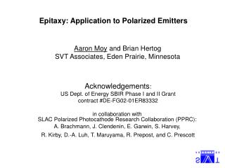
Epitaxy: Application to Polarized Emitters Aaron Moy and Brian Hertog SVT Associates, Eden Prairie, Minnesota Acknowledgements: US Dept. of Energy SBIR Phase I and II Grant contract #DE-FG02-01ER83332 in collaboration with SLAC Polarized Photocathode Research Collaboration (PPRC): A. Brachmann, J. Clendenin, E. Garwin, S. Harvey, R. Kirby, D.-A. Luh, T. Maruyama, R. Prepost, and C. Prescott
Outline • Strained Layer Semiconductor for Polarized Electron Source • Epitaxial Crystal Growth • Methods of III-V Epitaxy • Metal organic chemical vapor deposition (MOCVD) • Molecular beam epitaxy (MBE) • Gas source molecular beam epitaxy (GSMBE) • Growth of Photocathodes Using GSMBE • Characterization of Material
Polarized Electron Emitters • Emission of electrons with specific spin • Applications • High energy physics, colliders • Spintronics • Motivation • Efficiency ~ P2I, where P=polarization, I= current • Increased efficiency, less machine time cost
Strained Layer Polarized Emitters • Photocathode emission • Circularly polarized light • Unstrained GaAs • 50% max polarization • Compressively strained GaAs • lattice constant < 5.65 Å • valence band splitting • 3/2 1/2 transition favored • 100% max polarization
Creating Strained GaAs Layers • Heteroepitaxy • New layers will form based on previous lattice • Compressive strain • Growth on lattice with smaller lattice constant • Larger difference in lattice size increased strain force GaAs 5.65 Å GaAs0.64P0.36 5.58 Å Compressively strained GaAs on GaAs0.64P0.36 lattice constant 5.58 Å
Epitaxy Growth of thin film crystalline material where crystallinity is preserved, “single crystal” Atomic Flux Bare (100) III-V surface, such as GaAs Deposition of crystal source material (e.g. Ga, As atoms)
Epitaxy Result: Newly grown thin film, lattice structure maintained Starting surface
Epitaxy • Advantages of epitaxy- • Improved crystallinity • Reduced defects • Higher purity • Precise control of thickness • Precise control alloy composition • “Lattice matched” compounds • Abrupt or graded interfaces • Ability to engineer unique device structures • Nanostructures • Superlattices • Strained layers
III-V Compound Semiconductors III IV V VI VII VIII
How Epitaxy Is Achieved • Two primary methods for thin film epitaxy- • Metal Organic Chemical Vapor Phase Deposition (MOCVD) (aka metal organic vapor phase epitaxy MOVPE) • Molecular Beam Epitaxy (MBE) • Differences in growth chemistry
Metal Organic Chemical Vapor Phase Deposition • Growth in “reactor” • Pressure 10s-100s of torr • Metal organic group III source material • Trimethyl Gallium Ga(CH3)3 • Trimethyl Indium In(CH3)3 • MO vapor transported H2 carrier gas • Hydride group V source gas • Arsine AsH3 • Phosphine PH3 • Thermal cracking at growth surface
MOCVD- Surface Chemistry Surface chemistry- Basic layout of an MOCVD reactor
MOCVD Summary • Growth rates 2-100 micron/hr • high throughput • P-type doping • Zn (Diethyl Zinc), high diffusivity • C (CCl4, CBr4), amphoteric • Complex growth kinetics • delicate interaction between injected gasses, temperatures • High background pressure • Parasitic incorporation • Intermixing of atoms at interfaces
Molecular Beam Epitaxy (MBE) • Growth in high vacuum chamber • Ultimate vacuum < 10-10 torr • Pressure during growth < 10-6 torr • Elemental source material • High purity Ga, In, As (99.9999%) • Sources individually evaporated in high temperature cells • In situ monitoring, calibration • Probing of surface structure during growth • Real time feedback of growth rate
Molecular Beam Epitaxy Growth Apparatus
MBE- In Situ Surface Analysis • Reflection High Energy Electron Diffraction (RHEED) • High energy (5-10 keV) electron beam • Shallow angle of incidence • Beam reconstruction on phosphor screen RHEED image of GaAs (100) surface
MBE- In Situ Growth Rate Feedback Monitoring RHEED image intensity versus time provides layer-by-layer growth rate feedback
MBE- Summary • Ultra high vacuum, high purity layers • No chemical byproducts created at growth surface • High uniformity (< 1% deviation) • Growth rates 0.1-10 micron/hr • High control of composition • In situ monitoring and feedback • Mature production technology
Gas Source MBE • Combines advantages of MBE with gas source delivery of group V atoms (as used in MOCVD) • PH3, AsH3 used for group V sources • Thermally cracked at injector into P2, As2 and H2 • P2, As2 dimers arrive at growth surface along with Ga, In • MBE surface kinetics maintained
Gas Source MBE • Advantages of GSMBE • PH3 a more mature method for phosphorus MBE growth • Improved dynamic range of switching state • As, P molecules travel around shutter in solid source MBE • Control of P, As flux by adjustment of gas flow • Can replenish group V source material without breaking vacuum • Disadvantages • Requires gas handling system • Requires extra vacuum pumping to remove hydrogen • Arsine and Phosphine highly toxic
Limits to Strained Layers: Critical Thickness • Strain forces increase with thickness • Strain reaches threshold, lattice relaxes • “Critical Thickness” • Layer thickness where relaxation occurs • Relaxed lattice- bulk crystal state • Thickness inversely proportional to strain (difference in lattice constant) • Misfit dislocations created • Scattering, absorption of photons • Non-uniformities GaAs on GaAsP Critical Thickness
Photocathode Polarized Emitters • Device Considerations • Strained GaAs layer • Highly p-type doped • Thick to provide enough emission current • Structure Growth • Uniform • Excellent crystallinity • Substrate for epitaxy • High quality • Robust
Strained Superlattice Photocathode • Strained GaAs on GaAsxP1-x • Multiple GaAs layers sandwiched by GaAsxP1-x • Each GaAs layer below critical thickness • Multiple GaAs layers to provide thick overall active volume for electron emission • Superlattice- repetition of thin layers • GSMBE for epitaxy • Thin layers (< 50 Å) • Utilizes phosphorus • Abrupt, uniform interfaces
GaAsP 30 A Strained GaAs 30 A Active Region 1000 A GaAs0.64P0.36 Buffer GaAsP 2.5mm Strained GaAs GaAs(1-x)Px Graded Layer 2.5mm GaAsP Strained GaAs GaAs Substrate Strained Superlattice Photocathode x 16 pair
Strained Superlattice Photocathode by GSMBE • Growth details • Substrate heated to 580 °C to remove surface oxide • GaAs buffer layer grown at 1 micron/hr using AsH3 flow 3 sccm • GaAs -> GaAsP graded layer grown • Step graded GaAsxP1-x using six distinct compositions • Maintained AsH3 + PH3 = 4.5 sccm gas flow rate • GaAsP layer grown at 480 °C • Superlattice layer grown at 480 °C
Material Characterization- Photoluminescence Half die, PL points for uniformity probe
Conclusion • Strained layers for photocathode applications • Molecular beam epitaxy successful method for photocathode growth • MBE growth parameters and structure can be refined to improve polarization of devices