Download
1 / 52
540 likes | 843 Views
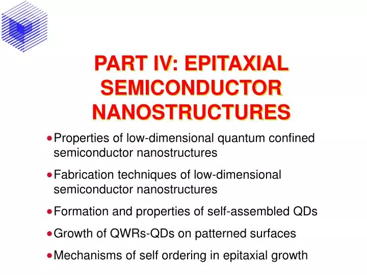
PART IV: EPITAXIAL SEMICONDUCTOR NANOSTRUCTURES. Properties of low-dimensional quantum confined semiconductor nanostructures Fabrication techniques of low-dimensional semiconductor nanostructures Formation and properties of self-assembled QDs Growth of QWRs-QDs on patterned surfaces

E N D
PART IV: EPITAXIAL SEMICONDUCTOR NANOSTRUCTURES Properties of low-dimensional quantum confined semiconductor nanostructures Fabrication techniques of low-dimensional semiconductor nanostructures Formation and properties of self-assembled QDs Growth of QWRs-QDs on patterned surfaces Mechanisms of self ordering in epitaxial growth
Properties of low-dimensional quantum confined semiconductor nanostructures
Effect of quantum confinement on energy spectrum • Energy spectrum for electrons confined in 1, 2 or 3D with infinitely deep, rectangular potential wells with sizes tx, ty, tz:
Electron DOS in low-D systems 3D - bulk 2D - QW 1D - QWR 0D - QD Lower D sharper DOS potential advantage for optical and electronic properties
Sizes needed to observe QC • At T = 0K electrons occupy all energy states up to EF, corresponding to de Broglie (Fermi) wavelength lF = 2p / (3p2n)1/3, with n = electron density. • Quantum confinement for ti≤ lF • Metals: 1 electron / atom lF≈ 0.5nm • Semiconductors: much higher, depends on doping: e.g., n~1X1018cm-3 lF= 29nm, ti ≈ 10nm is sufficient
Subband population in QC systems • If more subbands are populated, motion along confinement direction results only ground state must be populated, i.e., DE12 > kBT • For infinite square QW, this means • For electrons in GaAs at T = 300K tx < 20nm • For holes, more complicated relations and mh>me smaller tx • Equivalent sizes for other confinement dimensions
Uniformity requirements in QC structures • Size non-uniformity inhomogeneous broadening of DOS • For ∞ wells, |dEi|/ Ei = 2 dti / ti ; dEi << Ei dti << ti • Practical limit to observe QC: dti / ti < 10% dti ≈ 1nm Calculated electron DOS in a GaAs/AlGaAs QWR with different Gaussian-shaped inhomogeneous broadening
Fabrication techniques of low-dimensional semiconductor nanostructures
Control overlateral composition From Quantum Wells to Quantum Wires/Dots ? Planar (layer-by-layer) epitaxy QWR - QD QW
Main approaches for creation of lateral confinement • Top-down:Post growth patterning of epitaxially grown 2D quantum wells • Bottom-up:Formation of QWR / QD during growth by special epitaxial procedures
SEM image showing narrow pillars etched into a GaAs substrate. (horizontal bars = 0.5 mm(M. A. Reed et al., Phys. Rev. Lett. 60, 535 (1988)) Post-growth patterning 1 • Selective removal of QW by lithography, etching and regrowth • Lithography: holo, e-beam, X-ray • Etching: dry, wet depending on details of fabrication process • Regrowth: surface passivation Advantages: Flexibility of design (lithographic patterns) Disadvantages: Size: several 10nm Uniformity (size and shape): several nm Etching defects interface states 75-nmquantum wires fabricated in GaAs/AlGaAs material by e-beam lithography and chemical etching(M. L. Roukes et al. Phys. Rev. Lett. 59, 3011 (1987))
Post-growth patterning 2 • Selective disordering of QWs • Patterning of QW band gap and refractive index • Methods: implantation or diffusion of impurities through a mask or with focused ion beams Advantages: Flexibility of design (lithographic patterns) Disadvantages: Size: several 10nm Uniformity (size and shape): several nm Impurities material contamination
Post-growth patterning 3 • Deposition of patterned “stressors” adjacent to the QW • Lateral band-gap modulation via strain effects Advantages: Flexibility of design (lithographic patterns) Smooth, defect-free lateral interfaces Disadvantages: Size: several 10nm Uniformity (size and shape): several nm
Post-growth patterning 4 • Lateral patterning of 2D electron gas structures • Creation of QWRs, quantum point contacts (QPCs) and QDs • Methods: • Depletion by deposition of a metallic split-gate (top) • Wet chemical etching and depletion by in-plane gates (bottom) Advantages: Flexibility of design (lithographic patterns) Smooth, defect-free lateral interfaces Easy electric contacts Disadvantages: Size: several 10nm Uniformity (size and shape): several nm
Growth direction AlGaAs Growth direction GaAs AlGaAs GaAs Cleave here The process begins withthe usual growth of ahigh-mobility heterojunction After this the sampleis cleaved inside thevacuum chamber After cleavage the sampleis reoriented and growthis then resumed on topof the cleaved surface AlGaAs GaAs Cleaved-edge overgrowth • Overgrowth on the Cleaved (011) Edge of a (multiple) QW or 2DEG structure (CEO) • Cleave of the 2DEG in the MBE chamber • Overgrowth of 2DEG on topof the cleaved edge QWR at the point where the two 2DEGs intersect • lateral variation in the potential energy • 1 regrowth: QWRs; 2 regrowths: QDs A. R. Goni et al. APL. 61, 1956 (1992)
Cleaved-edge overgrowth W. Wegscheider et al. PRL 71, 4071 (1993) Advantages: Size, uniformity: ML scale Smooth, defect-free lateral interfaces Disadvantages: Low flexibility (difficult contacts on cleaved edge)
Spontaneous self-ordering 1 • Growth of fractional-layer SLs on vicinal substrates • Species-dependent surface diffusion and preferential attachment of adatoms to the step edges lateral and vertical definition, alignment • QWR formation: serpentine SL (growth rate modulations), accumulation at step bunches Advantages: 1-step process (no processing) Size: <10nm Lateral interfaces formed during growth Disadvantages: Uniformity: 10-20% (imperfect step configuration and spacing, incomplete adatom segregation, growth rate variations) Stacked GaAs/AlGaAs QWR SL formed on step bunches on 3o off (110) GaAs.(T. Kato et al., APL 72, 465 (1998)
Improvement: growth on misoriented substrates QD formation on quasi-periodic step edges Spontaneous self-ordering 2 • Stranski - Krastanov growth of QDs in lattice-mismatched system (e.g., InGaAs/GaAs) Advantages: 1-step process (no processing) Size: <10nm Lateral interfaces formed during growth Disadvantages: Uniformity: 10-20% in size and position (randomness of nucleation process) Difficult contacting for transport STM image of self-assembled InAs QDs on a GaAs substrate(M. E. Rubin et al. Phys. Rev. Lett. 77, 5268 (1996))
AlGaAs barriers GaAs QWR GaAs V-shapedsubstrate 100nm Seeded self-ordering • Growth of QWs on lithographically patterned substrates • Dielectric masks • Nonplanar surfaces • Mechanisms: selective (masks) or anisotropic (nonplanar) growth rates material accumulation on preferential sites (“seeds”) Advantages: Size: <10nm Uniformity: 5% (seeds) Lateral interfaces formed during growth Disadvantages: 2-step process (pre-patterning) Nanostructures depend on growth habit TEM X-section of a stack of GaAs/AlGaAs QWRs grown on a V-grooved substrate
Atomic arrangement in a QD High resolution TEM of an uncapped InAs/GaAs QD (Chu et al., JAP85, 2355 (1999)) The lateral lattice constant in the upper part of the QD is clearly larger than in the lower part: strain relaxation in the 3D island. When too much island material is deposited, the strain cannot be totally relieved elastically through islanding, and dislocations occur via plastic relaxation.
Self-limiting effect Formation stages of InAs/GaAs(001) QDs a) Low coverages: InAs step-flow growth. b)-c): ~1.7ML: pseudomorphic, defect free QDs, 10% uniformity. c): Higher density, smaller size than b). d)-f): >2ML: dislocated islands by QD aggregation or by dislocations in a single QD. 1X1mm2 AFM scans of different InAs coverages (1 to 4 ML) on GaAs (001) (Leonard et al., PRB 50, 11687 (1994))
Critical thickness for QD formation QD density = 0 below critical layer thickness QC Sharp density increase after QC QD density r = r0 (Q- QC)a, QC = 1.5ML, a = 1.76: 1st order phase transition with r an order parameter (Leonard et al., PRB 50, 11687 (1994))
1.6ML 1.65ML 1.75ML 1.9ML Size distribution of QDs Diameter and height distribution for increasing InAs coverage 10% height and 7% uniformity for initial stages of QD formation (a) Degraded uniformity for higher Q Increasing Q: diameter decrease (~30nm to ~ 20nm), density increase (Leonard et al., PRB 50, 11687 (1994))
Optical properties of QDs RT PL spectra for different Q 2-3 peaks corresponding to ground and excited states Size distribution of the QDs d-like DOS broad lines (inhomogeneous broadening) (Chu et al., JAP85, 2355 (1999))
Optical properties of QDs RT PL intensity, energy and FWHM as a function of Q Intensity: maximum for Q ~ 2.3ML Energy: broad minimum for Q ~ 2.3-2.7ML ( largest QDs) FWHM: minimum for Q ~ 2.6ML (30-35meV) larger islands: better optical quality, higher homogeneity Q > 2.7ML: formation of dislocations: decreased intensity, energy shift, broader lines. (Chu et al., JAP85, 2355 (1999)) Previous experiment: higher homogeneity, slightly higher size for lower Q (first stages of QD formation) high influence of experimental conditions!
Effect of growth temperature (MBE) (Chu et al., JAP85, 2355 (1999)) Increasing T (480-530C) decreasing energy larger QDs Explanation: larger diffusion length there is a larger nucleation-free area around islands ( nucleation centers, adatom sinks) where adatoms can be collected by the island 550C: In desorption (smaller QDs), In-Ga intermixing higher energy Increasing T: stronger, narrower lines better material quality Ground state – 1st subband separation (530C): ~ 70meV
Effect of V/III ratio (MBE) (Chu et al., JAP85, 2355 (1999)) T=480, different As4 flux: enhanced In diffusion for lower As4/In ratios Lower As4 fluxes:increased QD quantum efficiency Lower As4 fluxes: small redshift increased QD size ( larger diffusion length, coherent with T dependence)
Lithographic positioning of SA QDs • Self-assembled Ge islands on Si(001) pre-patterned with oxide lines • Increased uniformity in size and separation • Possible mechanisms: • Diffusion barrier on the stripe edge • Reduced strain energy at the stripe edge T. I. Kamins and R. S. Williams, APL 71, 1201 (1997)
Preferential formation of InAs QDs in shallow, sub-mm-size GaAs holes defined by electron-beam (a) 1.4ML, b) 1.8ML InAs) Holes with (111)A and B faces, QDs formed on B faces (favorable nucleation sites for In atoms). S Kohmoto, MSEB 88, 292 (2002) Lithographic positioning of SA QDs
Vertical stacking of QDs Coherent InAs islands separated by GaAs spacer layers exhibit self-organized growth along the growth direction. The island-induced evolving strain fields provide the driving force for self-assembly provided the spacer is not too thick Bright field TEM pictures taken along [011] azimuth of five sets of InAs islands separated by 36 ML GaAs spacer layers. Q. Xie et al., PRL 75, 2542 (1995) X-STM constant current topography image of two stacks of InAs QDs. D. M. Bruls et al., APL 82, 3758 (2003)
Lithographic positioning of stacked QDs Twofold stacked InGaAs/GaAs QD layers grown on GaAs(001) substrates patterned with square arrays of shallow holes ((a)(-d): 100-200nm period). The second QD layer responds to the lateral strain-field interferences generated by the buried periodic QD array: vertically-aligned QDs or satellite QDs placed on strain energy minima. Base size and shape, and lateral orientation are predefined by the Estr distribution on the underlying surface. H. Heidemeyer et al., PRL 91, 196103 (2003)
Stable facets forming in the groove: sidewalls:{111}A ~ 5-10° offtowards (100) top and bottom regions:(100) + {311}A (100) {311}A sidewalls {111}A GaAs substrate MOCVD on V-grooved substrates Different surface crystalline structure different diffusion & nucleation rates growth rate R depends on orientation Rtop, Rbottom < Rsidewall expansion at top, sharpening at bottom BUT: profile stabilizes at the bottom at the 10nm-level
QWR formation on V-grooved substrates AlGaAs self-limiting profile independent of lithographic details recovers after QWR deposition r ~ 10nm GaAs QW profile bottom region thickens and expands QWR formation AlGaAs vertical QW
Profile evolution during self-limiting growth G. Biasiol et al., APL 71, 1831 (1997). R(100) > R{ijk} conformal growth R(100) > R{ijk} (100) expanding layer A: t100 > t311 > tsexpansion of (100) and {311}A facets layer B: t100 = t311 = tsstable facets, self-limiting growth
Optical Properties of GaAs-AlGaAs QWRs* Photoluminescence Photoluminescence Excitation • hh and lh related transitions observed • polarization anisotropy in e-lh/e-hh ratio PL FWHM of QWR ~ 6meV *F. Vouilloz et al. ICPS 23, Berlin, 1996
Driving force for lateral epitaxy Chemical potential (driving force for epitaxy supersaturation): Lateral variations of m lateral variations of growth rate
Chemical potential growth rate Nernst-Einstein relation Continuity equation Diffusion towards areas of lower m Growth rate: increased at lower m, decreased at higher m
Example: sinusoidal chemical potential m(x) = sin (x) j(x) - m’(x) = -cos(x) R(x) m”(x) = -sin(x) j j j j
How self-ordering is established Need for an equilibrating action between non-uniform chemical potential (stress, shape, composition) and another factor that drives atoms away from chemical potential minima. As growth proceeds, this should bring to steady-state growth profile. Any change in growth parameters (materials, temperature, fluxes, growth rates...) should bring to a new steady-state profile, independent of the initial one.
Stressed surface self-ordering of QDs • SK growth mode: adatom flux towards islands island coarsening • Strain energy (chemical potential) Es: • Flux away from islands • Es larger for larger islands dissolution rate larger as island size increases • 1 + 2: kinetic mechanism stabilizing the island size: slowing of the growth rate of large islands and increase of the adatom density away from them, thus enhancing nucleation of new islands (with small Es faster growth). • narrow island size distribution in the system (for f = 5 and 7.5%). 1D KMC model, A.L. Barabasi, APL 70, 2565 (1997) f = 7.5% ()5 ()2.5% ()0% ()
Vertical self-ordering of stacked QDs Pairing probability between 1st and 2nd layer of dots decreases with thicker spacers Model: atoms of 2nd InAs layer arrive on stressed region (I) of width 2ls ( strain-driven diffusion towards top of 1st islands) or unstressed region (II) of width l-2ls ( random island formation) ls increases as GaAs spacer is thinner Surface diffusion model pairing probability as a function spacer thickness, dependent on island size and density (measured), lattice mismatch and strain (calculated) and In diffusion length LD (fit parameter) Very good match with exp data for LD = 280nm (@ T=400C) Full calculations in Q. Xie et al., PRL 75, 2542 (1995)
µt µs Ozdemir and Zangwill, JVSTA 10, 684 (1992) µb Diffusion towards the bottom Growth rate: increased at the bottom, decreased at the top Surface chemical potential on a patterned, faceted substrate lt lb
Growth rate anisotropy Mechanism of self-limiting growth Capillarity = Self-limiting growth G. Biasiol and E. Kapon, PRL 81, 2962 (1998),G. Biasiol et al., PRB 65, 205306 (2002).
AFM cross section of a V-groove AlxGa1-xAs heterostructure Ls(Ga) > Ls(Al) stronger Ga capillarity to the bottom Ga-rich AlxGa1-xAs vertical quantum well VQW Nonuniform composition ordered phase • increase of the entropy of mixing • to be included in the model Self-Limiting Growth: AlxGa1-xAs G. Biasiol and E. Kapon, PRL 81, 2962 (1998),G. Biasiol et al., PRB 65, 205306 (2002).
Composition dependence of self-limiting bottom widthEvidence for entropic contributions AlXGa1-XAs; T = 700°C fixed by experiment fitted, LsG=175±20nm G. Biasiol and E. Kapon, PRL 81, 2962 (1998),G. Biasiol et al., PRB 65, 205306 (2002).
Temperature dependenceArrhenius plots GaAs: AlXGa1-XAs: fit: EBG = 1.9±0.3eV fit: EBA = 2.3±0.2eV G. Biasiol and E. Kapon, PRL 81, 2962 (1998),G. Biasiol et al., PRB 65, 205306 (2002).