Download
1 / 92
920 likes | 1.2k Views
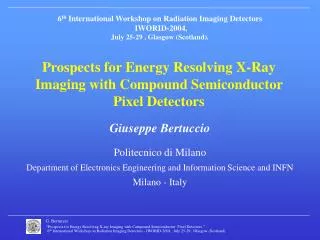
6 th International Workshop on Radiation Imaging Detectors IWORID-2004 , July 25-29 , Glasgow (Scotland). Prospects for Energy Resolving X-Ray Imaging with Compound Semiconductor Pixel Detectors. Giuseppe Bertuccio. Politecnico di Milano

E N D
6th International Workshop on Radiation Imaging Detectors IWORID-2004, July 25-29 , Glasgow (Scotland). Prospects for Energy Resolving X-Ray Imaging with Compound Semiconductor Pixel Detectors Giuseppe Bertuccio Politecnico di Milano Department of Electronics Engineering and Information Science and INFN Milano - Italy
Outline • GaAs and SiC X-Ray detectors
Outline • GaAs and SiC X-Ray detectors • The achieved results
Outline • GaAs and SiC X-Ray detectors • The achieved results • Some related issues : • Leakage current • Electronic noise • Charge transport
Outline • GaAs and SiC X-Ray detectors • The achieved results • Some related issues : • Leakage current • Electronic noise • Charge transport
Outline • GaAs and SiC X-Ray detectors • The achieved results • Some related issues : • Leakage current • Electronic noise • Charge transport • Prospects with GaAs and SiC pixel detectors
GaAs Radiation Detectors:30 years of a fascinating history • 1971-72 : Eberharth et al. (NIM-94), Kobayashi et al. (NIM-98) 1992 -1998: • Europe: Aachen, CERN, Freiburg, Glasgow, Imperial College, Lecce, Leicester, Milano, Modena, Pisa, Sheffield… • USA : Michigan Univ., Sandia; UCLA, Livermore, Naval, Berkeley, Wright Univ.
1996 – GaAs single pixel GaAs Politecnico di Milano – KFA Julich Collaboration MBE GaAs - 5 mm thick p-i-n structure (3·1014 cm-3) pixel: 170 x 320 mm Equivalent Noise Energies @ 20 °C: 532 eV FWHM (53 e- r.m.s.) @ -30°C: 373 eV FWHM (37 e- r.m.s.) IEEE Trans. Nucl. Sci. 44, 1997
2002 - Pixel Array A. Owen, M. Bavdaz, A. Peacock (ESA) S. Nenomen, H. Anderson (Metorex) G. Bertuccio, R. Casiraghi, D. Maiocchi (PoliMI) CVD GaAs - 40 mm thick p+n structure Pixel size: 200 mm x 200 mm
33 mm @ 100 V Equivalent to 20 X Silicon thickness (650 mm ) Epitaxial Layer Characteristics 1.5·1014 cm-3
pA Junction Leakage Current
3-12 nA/cm2 pA Junction Leakage Current
Can this current (noise) be lowered ? Room Temperature Soft Cooling IleakEquivalent Noise @ 5 ms 200 30
Leakage Current densities Is the ultimate limit reached for JGaAs ?
Investigation on the leakage curent origin in junctions on GaAs
Leakage current origin in GaAs detectors Schottky junction GaAs detectors
Leakage current origin in GaAs detectors Schottky junction GaAs detectors fB= 0.91 eV
Leakage current origin in GaAs detectors Schottky junction GaAs detectors fB= 0.91 eV
x 5 Leakage current origin in GaAs detectors Schottky junction GaAs detectors fB= 0.91 eV
Leakage current origin in GaAs detectors p+n junction GaAs detectors 291 K
Leakage current origin in GaAs detectors p+n junction GaAs detectors 291 K Thermal Generation EA = 0.7 eV tG = 1 ms
x 3 Leakage current origin in GaAs detectors p+n junction GaAs detectors Thermal gen. + Poole Frenkel effect 291 K Thermal Generation EA = 0.7 eV tG = 1ms
Leakage current in GaAs: conclusions • Current densities ≤ 10 nA/cm2 @ 290 K
Leakage current in GaAs: conclusions • Current densities ≤ 10 nA/cm2 @ 290 K • Schottky junction: • Barrier height f = 0.9 eV • Significant barrier lowering effects • Higher barrier, lower doping (smaller Em) required
Leakage current in GaAs: conclusions • Current densities ≤ 10 nA/cm2 @ 290 K • Schottky junction: • Barrier height f = 0.9 eV • Significant barrier lowering effects • Higher barrier, lower doping (smaller Em) required • p+n junction: • Generation current ( tG=1ms ; EA= 0.7 eV ) • Poole-Frenkel effect observed • Higher purity, lower doping (smaller Em) required
Prototype GaAs pixel array Test with discrete front-end electronics16 electrons r.m.s. at +20°C 14 electrons r.m.s. at -30°C
Thermoelectric cooling ( -30°C ) 163 eV FWHM (16 e - r.m.s.) Room temperature ( 20°C ) 242 eV FWHM (24 e - r.m.s.) GaAs pixel – best results Which are the limits ? Can we hope higher resolution ? Trans. Nucl. Sci. 50, 2003
Noise Components Analysis 20 °C GaAs detector connected Front-end electronics
Noise Components Analysis 20 °C GaAs detector connected Series noise Front-end electronics
Noise Components Analysis 20 °C GaAs detector connected Series noise Front-end electronics Current noise
Noise Components Analysis 20 °C GaAs detector connected Series noise Front-end electronics Current noise Dielectric noise
465 eV FWHM @ 59.5 keV (Fano limit: 410 eV FWHM) X-g Ray Spectroscopy with GaAs T = -30°C ENE = 204 eV FWHM ( 20 e- r.m.s.)
241Am 59.54 keV 501 ± 5 eV FWHM Pulser 283 ± 1 eV FWHM 59.5 keV line analysis 20 °C Is the Charge Collection Efficiency 100 % ? • No significant charge trapping • Fano factor : F = 0.124 ± 0.004
Accurate knowledge of the electron-hole pair generation energy required Charge trapping in GaAs detectors
Generation Energy in GaAs e = 4.55 – 0.00122 T [eV] 300 K : e = 4.18 ± 0.02 eV Bertuccio, Maiocchi, JAP 92, 2002
CCE ≥ 99 % le+ lh= 1400 mm @ 110 V Charge Collection Efficiency
Conclusions on tested GaAs pixel • High resolution with epi-GaAs pixels • 242 eV FWHM @ 20°C • 163 eV FWHM @ -30°C
Conclusions on tested GaAs pixel • High resolution with epi-GaAs pixels • 242 eV FWHM @ 20°C • 163 eV FWHM @ -30°C • Main noise component: dielectrics (with discrete electronics)
Conclusions on tested GaAs pixel • High resolution with epi-GaAs pixels • 242 eV FWHM @ 20°C • 163 eV FWHM @ -30°C • Main noise component: dielectrics (with discrete electronics) • Leakage current density: ≤ 10 nA/cm2 @ 20°C
Conclusions on tested GaAs pixel • High resolution with epi-GaAs pixels • 242 eV FWHM @ 20°C • 163 eV FWHM @ -30°C • Main noise component: dielectrics (with discrete electronics) • Leakage current density: ≤ 10 nA/cm2 @ 20°C • Mean drift length: up to 1.4 mm (CCE>99 % for 30 mm)
Conclusions on tested GaAs pixel • High resolution with epi-GaAs pixels • 242 eV FWHM @ 20°C • 163 eV FWHM @ -30°C • Main noise component: dielectrics (with discrete electronics) • Leakage current density: ≤ 10 nA/cm2 @ 20°C • Mean drift length: up to 1.4 mm (CCE>99 % for 30 mm) • Limits: depletion layer depth (detection efficiency) • residual doping 1014 cm-3 • Epi layer thickness: 40 mm
GaAs pixel detectors Status • Good Schottky and p+n junction detectors exists ! • Epitaxial thickness >300 mm has been grown (Poster: Glasgow-Paris)
GaAs pixel detectors Status • Good Schottky and p+n junction detectors exists ! • Epitaxial thickness >300 mm has been grown (Poster: Glasgow-Paris) Prospects • Energy resolution of 180 eV FWHM are reachable at 20°C • Residual doping ≤1013 cm-3 required • Integrated spectroscopic-grade front-end electronic required
GaAs pixel detectors Status • Good Schottky and p+n junction detectors exists ! • Epitaxial thickness >300 mm has been grown (Poster : Glasgow-Paris) Prospects • Energy resolution of 180 eV FWHM are reachable at 20°C • Residual doping ≤1013 cm-3 required • Integrated spectroscopic-grade front-end electronic required
A Finmeccanica Company Large Format Detector Readout ASIC D. Martin, A. Owens EUROPEAN SPACE AGENCY, ESA-ESTEC - Noordwjik (NL) P. Bastia, I. Cappelluti, F. Ferrari, N. Ratti ALENIA SPAZIO s.p.a. - LABEN - MILANO ( I ) P. Malcovati, F. Borghetti, V. Ferragina PAVIA UNIVERSITY ( I ) G. Bertuccio, S. Caccia, D. Maiocchi, A. Pullia POLITECNICO DI MILANO ( I ) Supervision Readout system & coordination Back-end design Front-end design
250 m Design goal E=180 eV @ 5.9 keV LFDR ASIC for GaAs Pixels GaAs 32 x 32 array 1.2 cm 1.2 cm
A Finmeccanica Company LFDR ASIC (designed – in production) • 0.35 mm CMOS (AMS) • 16 x 16, 32x32, 64x64 pixel channels • 300 x 300 mm2 channel size • Complete: Preamplifier ADC • Spectroscopic grade - 500 mW/channel (simulated) • 30 electrons r.m.s. @ 20°C (simulated)
LFDR : ASIC Block diagram ADC’s cell’s registers analog cells 16x16 - 64x64 I/O- Interfaces