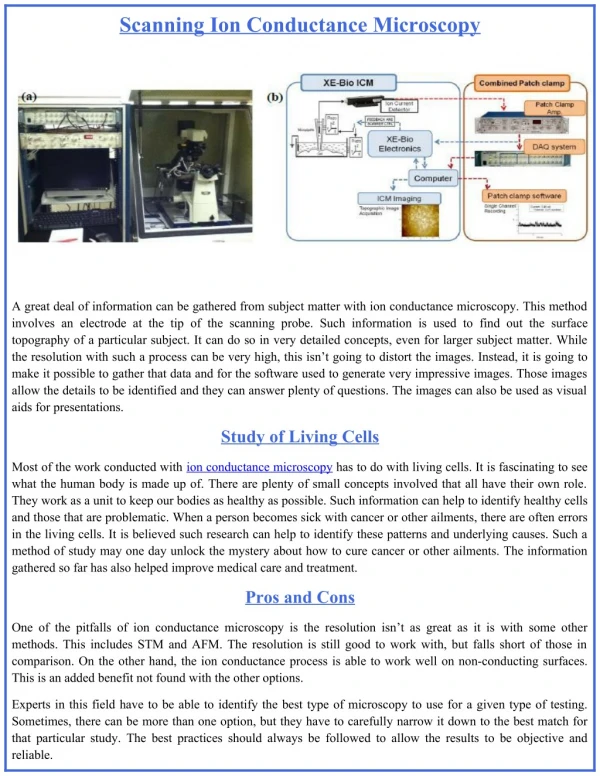
Download
1 / 18
190 likes | 215 Views
Explore the intricate workings of an SEM, its relevance to industry, and the impact of simulation methods on measurement accuracy and model optimization in industrial microscopy applications. Learn about simulations of electron scattering phenomena, sample shapes, and detection algorithms. Discover how modeling aids in critical dimension, defect, and contour metrology.

E N D
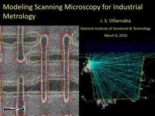
Modeling Scanning Microscopy for Industrial Metrology J. S. Villarrubia National Institute of Standards & Technology March 9, 2010
This talk is about • What goes on in an SEM? • How is this relevant to PED’s mission and to industry? • Impact of our work
Electrons scatter within a finite “interaction volume.” The size of this volume is related to —signal level —spatial res. —edge bloom size —topographic contrast An SEM animation: Electron gun Electron optical column SE Detector Fast (E>50 eV) backscattered electrons Sample We simulate all of these phenomena using Monte Carlo methods.
Our simulator (JMONSEL) allows samples to have complicated 3-dimensional shapes.
+Z Nucleus electron e Within each region we simulate the main scattering phenomena: 1. Elastic scattering
electrons Within each region we simulate the main scattering phenomena: 2. Secondary electron generation + nucleii SE generation via a plasmon intermediary SE generation by impact scattering
Within each region we simulate the main scattering phenomena: 3. Interface scattering Inside Outside An electron must “go uphill” to get out of the sample. Sometimes it bounces. (Transmission probability < 1.)
To write our simulator, we take advantage of NIST strengths. Our division, PED, has a long history of involvement in modeling the SEM, AFM and Optics. JMONSEL, is an outgrowth of our earlier MONSEL program. We collaborate with NIST’s Microanalysis Division (who have vast experience in modeling x-ray scattering . There is a little overlap in the physics, but a lot in 3-D sample shapes. For our secondary electron generation model, we use methods proposed and developed by Cedric Powell and David Penn (Physics Lab). Much of our input data is the same input data used for NIST Standard Reference Database 71 (Electron Inelastic Mean Free Paths). Our elastic scattering model is based on NIST Standard Reference Database 64 (Electron Elastic Scattering Cross Section Database).
How is this relevant to PED’s mission and to industry? In general Example 1: Critical dimension metrology Example 2: Defect metrology Example 3: Contour metrology
Generally: At least 3 kinds of questions that require modeling frequently arise in industrial microscopy: • What am I looking at? —Does this shape or this one go with • How do I optimize my measurement? —What instrument settings for best topographic contrast? — How about best material contrast? — What about highest resolution for given throughput? • What are the limits? —If an electrical contact were broken at the bottom (sub-surface) would its image look any different? —If I could make a transistor gate this small, would I be able to measure it? Measurement
To answer these questions, the tool’s image is not enough. Questions about image interpretation (especially quantification) require us to decide whether the image we have is consistent with this or that instrument state (e.g. beam size & shape) & sample state (e.g., feature size & shape). For optimization, we want to know how the image would change if we changed instrument settings. Questions about limits often arise when the image shows nothing—and we want to know: would we see X if it were there? We need the image AND a model.
w e e w – 2e Example 1: Modeling assigns edge positions for nanometer-scale critical dimension metrology -?- -?- Where are the edges? With what uncertainty?
Example 2: JMONSEL is simulating industrial defect test samples to assist defect detection Intentional defect array sample modeled at SEMATECH request. Measurement JMONSEL Simulation Uses: (1) Answer questions about limits of detection. (2) Help design and optimize detection algorithms.
Example 3: JMONSEL has identified a measurement artifact in contour metrology Contours of constant brightness This effect has since been observed experimentally. Shift These brightness contours shift ~1.5 nm when they move from isolated to dense neighborhood. These are 30 nm lines and spaces.
Examples from AFM and Statistics work: AFM: We developed, published, and posted software for modeling Atomic Force Microscopy. • The methods are now in widespread use. • One of our papers on the subject has been cited 182 times and counting. • Citing papers document uses in • CD metrology • Nanoscale mechanical characterization by nanoindentation • Characterization of biological materials • Surface roughness metrology • Studies of crystallization and melting in polymers • Tribology • … Statistics: We alerted the industry to a bias error in linewidth roughness measurement and proposed a solution. • The original paper was “Best metrology paper of 2005” (SPIE) • All major CD-SEM suppliers now use unbiased metrics.
Examples from SEM simulation work of this project: Our earlier SEM code (MONSEL) is being used by: • — at least 5 semiconductor electronics manufacturers, • — 5 instrument suppliers, and • — 7 universities or research institutes. One CD-SEM vendor sent a guest researcher to work with us. We continue to interact. A (Model-Based Library) method we developed to enable model results to be applied to metrology was recipient of Nanotech Briefs Nano50 award in 2005. Our ongoing work is partially funded by International SEMATECH (a semiconductor industry consortium). New code to be released December 2010. Questions?