Download
1 / 14
140 likes | 164 Views
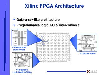
Design of Next-Generation FPGA w ith Hierarchical Interconnect Architecture. Cheng C. Wang, Fang-Li Yuan, Henry Chen, Rashmi Nanda, and Chia-Hsiang Yang Advisor: Prof. Dejan Markovic. ′. Introductions. Xilinx Virtex, Altera Stratix, etc. 2-D mesh network: O(N 2 )

E N D
Design of Next-Generation FPGA with Hierarchical Interconnect Architecture Cheng C. Wang, Fang-Li Yuan, Henry Chen, Rashmi Nanda, and Chia-Hsiang Yang Advisor: Prof. Dejan Markovic ′
Introductions • Xilinx Virtex, Altera Stratix, etc. • 2-D mesh network: O(N2) • Unconstrained I/O pins of CLB • 40~65-nm, full-custom SRAM • Proposed approach • Hierarchical network: O(Nlog2N) • 6-pin LUT (4 in, 2 out); 4 LUTs/CLB • 65-nm standard-cell flip-flops • Based on feature set of modern Xilinx FPGAs • Structure of CLB • Two types of SLICEs (L & M)
Architecture of SLICE in CLB • Configuration block (CB) • Look-up table (LUT); Carry chain (CY); Arithmetic function; Output stage (OP) • Logic unit (LU) = LUT + CY + OP • Total of 16 inputs & 8 outputs per SLICE
Look-up Table • Gated clock for CB and LUT • Only active in configuration phase • Two modes supported by LUT • One 4-input or Two 3-input functions • Two functions w/ 4 inputs if overlap • Suitable for Group P/G in adder design
What’s More in SLICE M • LUT/Mem. Combination • Four → Five/Six-input • Flexible mem. architecture • Seven modes • Write-signal gen.
What’s More in SLICE M • LUT/Mem. Combination • Four → Five/Six-input • Flexible mem. architecture • Seven modes • Write-signal gen.
Some Numbers in 65-nm Process • No longer need reg.-file for configuration scan-chain • DFFQNX2: 2.0x4.4 um2 v.s. RF1R1WSX1P4: 2.0x4.0 um2 • Minor area reduction but not safe • Circuit characteristic extraction (synthesis) • 90-nm v.s. 65-nm • 50% area • 70% delay • 74% energy
Design Example: 16-bit Adder • Model for rapid performance estimation of given spec. • Delay performances among RC and CLA intersect @ 64-b • RC: 10x area, 5.6x energy & 1.8x speed gap to ASIC • CLA: 50x area, 30x energy & 2.3x speed gap to ASIC
Dedicated DSP Block: Multiplier • 8x8 signed/unsigned multiplier • Large-size MUL • Combination with CLB or dedicated addition stage
Baugh-Wooley Multiplier • Support both signed/unsigned operations • General form • Example: 4x4
Putting it all Together • 8x8 multiplier: 850 um2; 0.23 pJ • SLICE L: 1600 um2; 0.89 pJ • SLICE M: 2700 um2; 1.38 pJ • Switch matrix (SM): 90 um2; 0.04 pJ • Switch box (SB):74 um2; 0.016 pJ (estimated) • Roughly, 1 SLICE L = 2 MUL • 1024-LUT Hier. • 192 L + 64 M + 10240 SM = 1.6 mm2; 0.7 nJ • full connectivity • 1024-LUT 2-D (32-LUT 2-D x 32 cores) • 192 L + 64 M + 131072 local SB + 16384 Global SB = 11 mm2; 2.6 nJ • <10% connectivity