s b
230 likes | 375 Views
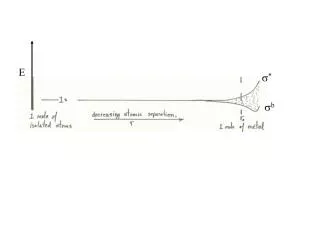
E. s *. s b. E. Looking only at this region in the Rectangle:. We generated a Band Diagram. If we include the relative number of orbitals, we make a Density of States DOS Diagram. We generated a Band Diagram.

s b
E N D
Presentation Transcript
E s* sb
Looking only at this region in the Rectangle:
We generated a Band Diagram If we include the relative number of orbitals, we make a Density of States DOS Diagram
We generated a Band Diagram If we include the relative number of orbitals, we make a Density of States DOS Diagram
We do the same thing again, starting with isolated atoms, Then turn on the bonding, then increase the number of interactions.
P Mn Mn Polymeric unit P
An actual example, calculated using an M.O.theory %Mn in orbital (state) %P in orbital (state) P Mn Mn Polymeric unit P
Using Band Diagrams: Conductivity • Conductivity - in two flavors • 1. Electronic conduction - electrons move • typical of metals; • example: Cu and Al very good • conductivity “predicted” by band diagrams • 2. Ionic conduction - ions move • requires “ionic” material • requires defects: vacancy and interstitial • (Schottky and Frenkel types) • example: AgI2 and HgM2I4
Semi Conductor Insulator MOT analogies with Band Diagram - HOMO / LUMO and type of reactivity - Valence Band / Conduction band and - DE and Band Gap MetallicConductor Empty bands small band gap Large Band Gap conduction band no band gap valence band filled bands
More typically simplified to show only “frontier” bands: MetallicConductor Semi Conductor Insulator conduction band Fermi level ef no band gap Large Band Gap small band gap ef ef valence band DE < 10 kJ/mol DE ~ 10 -100 kJ/mol DE > 400 kJ/mol
How Defects Improve Semi-Conduction Pure Germanium Gallium-Doped Ge Ga more Electropositive: Adds “Orbitals” At Higher Energy With Fewer Electrons Pure Ge Band Gap small band gap Gallium-Doping creates positive holes, as an acceptor band: DE ~ 0.66 eV A p-type semi-conductor
How Defects Improve Semi-Conduction Arsenic-Doped Ge Pure Germanium As is more Electronegative: Adds “Orbitals” At Lower Energy Partially Filled with Electrons small band gap Pure Ge Band Gap Arsenic-Doping creates negative holes, as a donor band DE = 0.66 eV An n-type semi-conductor
How Defects Lead to Devices PN Junctions = Diodes n-type p-type Fermi level in n-type semi-conductor is at higher energy than for the p-type: Spontaneous flow of electrons in one direction only. ef small band gap ef Directional Flow of electrons --> current goes in one direction only
In a pn junction, current spontaneously flows in one direction
How Defects Lead to Devices Band Gap threshold can be exceeded by: energy as light - photoconductivity devices: - photocells, photovoltaic cells (GaAs) - solar cells (Si) - pn-junctions with suitable ef make Light Emitting Diodes (LED) energy as heat – thermoconductivity devices: - thermistors
How Defects Lead to Devices: Photocopy (Xerox) Process (photolithography) - uses photoconductivity of Selenium Se paper w/ image Se Ink (toner) Se
How Defects Lead to Devices: Thermochromic Materials - example based on HgM2I4 materials
Replace S with I, Zn (at vertices) with Hg Zn (in middle) with Ag Prototype Cubic ZnS (zinc blende), two adjacent cells Replace S with I, Zn (at vertices) with Hg, Zn (in middle) with Cu
How Defects Lead to Devices: Thermochromic Materials - example based on HgM2I4 materials - adding energy as heat creates defects Cu(+) vacancies (Schottky defects) and interstital sites (Frenkel defects) - defects change band gap, change color, change conductivity