Download
1 / 12
130 likes | 199 Views
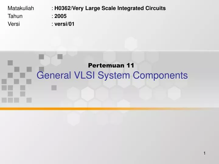
Pertemuan 11 General VLSI System Components. Matakuliah : H0362/Very Large Scale Integrated Circuits Tahun : 2005 Versi : versi/01. Learning Outcomes.

E N D
Pertemuan 11General VLSI System Components Matakuliah : H0362/Very Large Scale Integrated Circuits Tahun : 2005 Versi : versi/01
Learning Outcomes Pada Akhir pertemuan ini, diharapkan mahasiswa akan dapat menerapkan gerbang logik, switching logik, dan atau struktur deskripsi Verilog untuk membangun rangkaian sederhana dengan level hirarki lebih tinggi dalam CMOS VLSI.
s s p0 f Verilog HDL: p0 f module simple_mux (mux_out, p0, p1, select) ; input p0, p1 ; input select ; output mux_out ; always @ (select) ; case (select) 1’b0: mux_out = p0 ; 1’b1: mux_out = p1 ; endcase endmodule p1 p1 f = p0 . s + p1 . s Multiplexor Multiplexor 2:1 n: number of input f : output m: number select n = 2m Gate level multiplexor:
s s p0 f p0 p1 f s p1 Multiplexor Multiplexor 2:1 Implementasi rangkaian multiplexor 2:1 dapat juga dilakukan dengan rangkain logic switch sehingga Verilog HDL nya juga akan berubah. Cara lain Gate level multiplexor:
Verilog HDL: s0 module bigger_mux (out_4, p0, p1, p2, p3, s0, s1) ; input p0, p1, p2, p3 ; input s0, s1 ; output out_4 ; assign out_4 = s1 ? (s0, p3 : p2) : (s0 ? p1 : p0) ; endmodule s1 p0 0 1 p1 f 0 s0 1 p2 0 1 p3 Multiplexor Multiplexor 4:1 Gate level multiplexor:
Verilog HDL: module gate_mux_4 (out_gate, p0, p1, p2, p3, s0, s1) ; input p0, p1, p2, p3 ; input s0, s1 ; wire w1, w2, w3, w4 ; output out_gate_4 ; nand (w1, p_0, ~s1, ~s0), (w2, p_1, ~s1, s0), (w3, p_2, s1, ~s0), (w4, p_3, s1, s0), (out_gate, w1, w2, w3, w4) ; endmodule Multiplexor 4:1 s1 s0 Cara lain p0 s0 s1 p1 f p0 f 0 p2 p1 1 p2 2 p3 3 p3 f = p0 . s1 . s2 + p1 . s1 . s0 + p2 . s1 . s0 + p3 . s1 . s0 Multiplexor Gate level multiplexor:
Verilog HDL: module tg_mux_4 (f, p0, p1, p2, p3, s0, s1) ; input p0, p1, p2, p3 ; input s0, s1 ; wire w0, w1, w2, w3, w_0, w_x ; output f ; nmos (po, w0, ~s1), (w0, w_0, ~s0) ; nmos (p1, w1, ~s1), (w1, w_0, s0) ; nmos (p2, w2, s1), (w2, w_0, s0), nmos (p3, w3, s1), (w3, wp_0, s0) ; not (w_x, w_0), (f, w_x) ; endmodule Multiplexor 4:1 Cara lain s0 s1 s2 s3 p0 p1 f p2 p3 Multiplexor Gate level multiplexor:
Verilog HDL: module decode_4 (d0, d1, d2, d3, s0, s1) ; input s0, s1 ; ouput d0, d1, d2, d3 ; nor (d3, ~s0, ~s1), (d2, s0, s1), (d1, s0, ~s1), (d0, s0, s1) ; endmodule do = s1 . s0 = s1 + s0 d1 = s1 . s0 = s1 + s0 d0 d1 d2 d3 d2 = s1 . s0 = s1 + s0 s1 s0 d3 = s1 . s0 = s1 + s0 s0 s1 0 1 2 3 2/4 s1 s0 d0 d1 d3 d4 0 0 1 0 0 0 0 1 0 1 0 0 1 0 0 1 0 0 1 1 0 0 0 1 d0 d1 d2 d3 Binary Decoders 2/4 decoder Gate level multiplexor:
Verilog HDL: module d_latch (q, q_bar, d) ; input d ; ouput q, q_bar ; reg q, q_bar ; always @ (d) ; begin (t_d) q = d ; (t_d) q_bar = ~d ; end endmodule VDD Q D Q Q D Q Q Q D Diagram logik simbol Rangkaian CMOS Latch module d_latch_gates (q, q_bar, d) ; input d ; ouput q, q_bar ; wire not_d ; not (not_d, d) ; nor (t_nor) g1 (q_bar, q, d), (t_nor) g2 (q_bar, not_d) ; endmodule Gate level latch:
Verilog HDL: module d_latch (q, q_bar, d, enable) ; input d, enable ; ouput q, q_bar ; reg q, q_bar ; always @ (d and enable) ; begin (t_d) q = d ; (t_d) q_bar = ~d ; end endmodule Q D D Q Q En Q En simbol Diagram logik Latch Gate level latch:
Verilog HDL: module positive_dff (q, q_bar, d, clk) ; input d, clk ; ouput q, q_bar ; reg q, q_bar ; always @ (posedge clk) ; begin q = d ; q_bar = ~d ; end endmodule M3 M1 D Q Q Master Slave M2 M4 Positive edge 1 Load Master Transfer to slave t 0 0 T D Flip Flop Master Slave D Flip-Flop Positive-edge Gate level:
RESUME • Multiplexor. • Binary Decoders. • Latch. • D Flip Flop