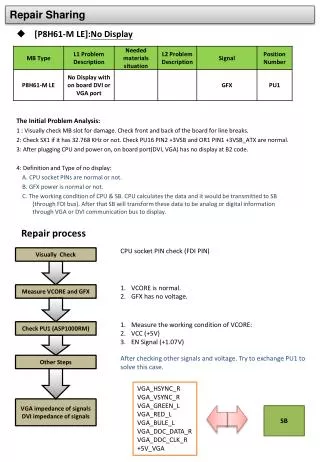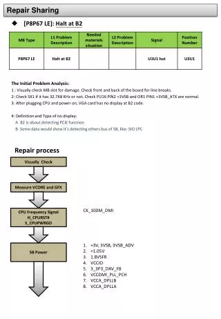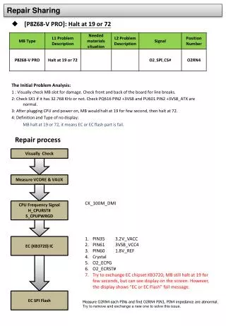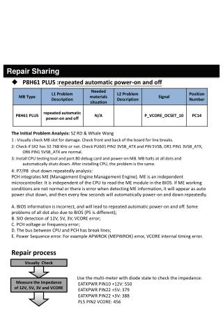
Repair Sharing
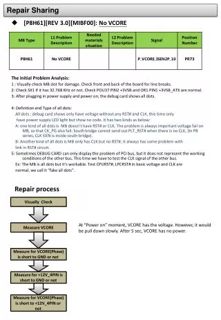
Repair Sharing. P8Z68-V PRO : All dots The Initial Problem Analysis: 1 : Visually check MB slot for damage. Check front and back of the board for line breaks. 2: Check SX1 if it has 32.768 KHz or not. Check PU601 PIN2 3VSB_ATX and PQ616 PIN2 3VSB are normal.

Repair Sharing
E N D
Presentation Transcript
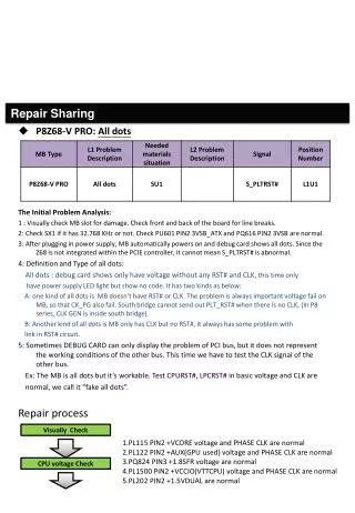
Repair Sharing • P8Z68-V PRO: All dots • The Initial Problem Analysis: 1 : Visually check MB slot for damage. Check front and back of the board for line breaks. 2: Check SX1 if it has 32.768 KHz or not. Check PU601 PIN2 3VSB_ATX and PQ616 PIN2 3VSB are normal. • 3: After plugging in power supply, MB automatically powers on and debug card shows all dots. Since the Z68 is not integrated within the PCIE controller, it cannot mean S_PLTRST# is abnormal. • 4: Definition and Type of all dots: • All dots : debug card shows only have voltage without any RST# and CLK, this time only • have power supply LED light but show no code. It has two kinds as below: • A: one kind of all dots is MB doesn’t have RST# or CLK. The problem is always important voltage fail on MB, so that CK_PG also fail. South bridge cannot send out PLT_RST# when there is no CLK, (In P8 series, CLK GEN is inside south bridge). • B: Another kind of all dots is MB only has CLK but no RST#, it always has some problem with • link in RST# circuit. • 5: Sometimes DEBUG CARD can only display the problem of PCI bus, but it does not represent the working conditions of the other bus. This time we have to test the CLK signal of the other bus. • Ex: The MB is all dots but it’s workable. Test CPURST#, LPCRST# in basic voltage and CLK are • normal, we call it “fake all dots”. • Repair process Visually Check 1.PL115 PIN2 +VCORE voltage and PHASE CLK are normal 2.PL122 PIN2 +AUX(GPU used) voltage and PHASE CLK are normal 3.PQ824 PIN3 +1.8SFR voltage are normal 4.PL1500 PIN2 +VCCIO(VTTCPU) voltage and PHASE CLK are normal 5.PL202 PIN2 +1.5VDUAL are normal CPU voltage Check 1
1.SR217,SR216,SR218 PIN1 and 2 +1.8SFR are normal , value is 1.8V. 2.SR225 +1.8V_NV_IO are normal. 3.PL502 +1.05PCH Voltage and PHASE CLK are normal 4.SR536 +1.05ME is normal 5. SR228 +1.05PCH_SRC is normal 6.SD1+BAT_3V is normal 7.SR222 +3VSB_SB is normal 8.PQ616 PIN2 +3VSB is normal PCH(Z68) supply check PCH Integrated CLK GEN Check if PCH CLK GEN works as normal 1.SR501 PIN1 S_25M_IN 2.SR501 PIN2 S_25M_OUT 3.SR553 PIN1 C_PCI_PCH 33M 4.SR552 PIN1 C_PCI_SIO 33M 5.SR555 PIN1 C_48M_SIO 48M 6.SR551 PIN1 C_PCI_EC 33M 7.SR554 PIN1 C_PCI_ASM1085 33M 8.K1C502,K1C501 PIN2 C_PCIE_K1, C_PCIE_K1# 100M Please refer other CLK which from PCH CLK GEN If the CLK are normal, it means problem is all dots only have CLK but no RST#. External frequency Storage device Check if External CLK GEN works as normal 1.OLP3 PIN2 +3V_CLK_BUF 2.CU2 PIN1,2 C_PCIE_X1_BUF,C_PCI_X1#_BUF 100M 3.CU2 PIN6,7 C_PCIEX1_1_R,C_PCIEX1_#1_R 100M 4.CU2 PIN9,10 C_PCIEX1_2_R,C_PCIEX1_#2_R 100M 5.CU2 PIN23,22 C_PCIE_U3A_R,C_PCIE_U3A#_R 100M PWROK(GD) 1.ORN214 PIN8 B_ATX_PWROK 3V 2.SR224 PIN2 S_DPWROK 3V 3.OR605 PIN1 O_PWROK_SIO 3V 4.SR518 PIN1 O_PWROK 3V 5.SR518 PIN2 S_MEPWROK_PCH 3V 6.SD5 PIN2 VRMPWRGD 3V 7.SR98 PIN2 S_DRAMPWRGD 1.5V 8.SR12 PIN1 H_CPUPWRGD 1V S_PLTRST# Check K1C19 S_PLTRST# is only 1.5V. Normal is 3V, but PCH had changed. So confirm PCH voltage and CLK, power GD are normal. Refer to the pcbrepair; there are some IC chip connect signal S_PLTRST#, such as O2U1(EC), OU1(SIO), K1U1(PCI chip) T1U1(SATA), U3QU1(USB3.0), U3U1(USB3.0), L1U1(LAN), touch the chip and check all the temperature are normal. 1.O2L1 PIN1 +3VSB_VCC4 2.O2U1 PIN6,18,54 +3VSB 3.O2X1 PIN1,2 32.768KHz 4.O2U2(EC BIOS) PIN1 O2_SPI_CS#_Q(check if there have a jump to get down ) O2U1(EC)
OU1(SIO) 1.OU1 PIN46,85 +3VSB_ATX 2.OU1 PIN1,24,106 +3V 3.OU1 PIN99 +BAT_3V K1U1(PCI CHIP) 1.PU503 PIN4 +K1_1.2V 2.K1L1 PIN2 +K1_1.2V_P 3.KIU1 +3V T1U1(SATA) T1R1 PIN1and2 25MHz T2U2(SATA) T2R2 PIN1and2 25MHz U3C60,U3C61 PIN1 20MHz U3U1(USB3.0) U3QU1(USB3.0) U3QR30 PIN1,2 20MHz L1U1(LAN) 1.L1C8 ,L1C7 PIN1 25MHZ fail 2.PQ855 PIN2 +3VSB_DUAL_LAN is normal 3.L1L1 PIN1 VDD1P0 don’t have voltage and CLK. Make sure L1U1 works abnormal, move L1U1,MB is OK. Note: LAN RST signal S_PLTRST# is from PCH.(not SIO)