Download
1 / 25
260 likes | 474 Views
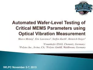
Automated Wafer-Level Testing of Critical MEMS Parameters using Optical Vibration Measurement. Marco Meinig 1 , Eric Lawrence 2 , Steffen Kurth 1 , Heinrich Steger 3 1 Fraunhofer ENAS, Chemnitz, Germany; 2 Polytec Inc., Irvine, CA; 3 Polytec GmbH, Waldbronn, Germany. Outline.

E N D
Automated Wafer-Level Testing of Critical MEMS Parameters usingOptical Vibration Measurement Marco Meinig1, Eric Lawrence2, Steffen Kurth1, Heinrich Steger31Fraunhofer ENAS, Chemnitz, Germany; 2Polytec Inc., Irvine, CA; 3Polytec GmbH, Waldbronn, Germany
Outline • Introduction: Measurement tasks in the MEMS field • Optical Vibration Measurement with Laser-Doppler Vibrometry • Parameter Identification by Vibration Measurement • MEMS test procedures using LDV • Examples
Introduction • Fabrication of MEMS is subject to process variations • Critical parameters are e.g. thickness, width or stress • Deviations lead to a certain amount of defective devices • Identification at wafer level saves costs (e.g. packaging ) • Existing technologies are not generally suitable for wafer level test
Introduction • A test method should be suitable for • Wafer level tests in the fabrication line • The cleanroom environment • Tests of 100 % of the fabricated devices • Requirements are • Time efficiency • Non-destructive measurement • Non-contact measurement technique Prober with vibrometer Vacuum prober WLI
Introduction • Challenges for non-electrical testing are • High spatial resolution, accuracy and precision • High bandwidth for fast system response • Wide range of performance criteria among different devices • Handling and environment requirements • High speed measurement in the fabrication line • Reliable techniques that allow scientists and engineers to effectively communicate physical properties
f0 f0 ± fD Bragg cell Measurement Beam He-Ne Laser <1mW (633nm) Reflected Beam x(t) v(t) f0 + 40 MHz Photo-detector Frequency Modulated Signal 40 MHz ± fD The Heterodyne Interferometer Δ fD = 2v/λ
MSA Micro System Analyzer withScanning Laser-Doppler Vibrometer • The interferometer is coupled via a fiber into the microscope (MSA) • Scanning mirrors allow to scan the whole surface point by point • Easy integration into Probe Stations
MSA Micro System Analyzer • The MSA-500 is an All-in-One optical MEMS Measurement Workstation forStatic and Dynamic Analysis • OOP Out-of-plane vibration measurement • IP In-plane vibration measurement • Frequency response, deflection shapes, switching response, damping response, ... • Static surface topography measurement • Form, Flatness, Smoothness/Roughness, Tilt, Profile
More Solutions forMicroStructures • The MSA-100-3D for real-time 3D vibration analysis with sub-pm resolutionfor all 3 axis • UHF Vibrometer for microscope-based vibration measurement up to 1.2 GHz • Compact Single Point Vibrometers for fast wafer-level test applications
Parameter identification by vibration analysis a) Theoretical route to vibration analysis Description of Structure VibrationModes ResponseLevels Spatial Model (mass, damping,stiffness) Modal Model (natural frequency,modal damping,mode shape of vibration) Response Model (impulse response,frequency response) Certain parameters b) Experimental vibration/modal analysis VibrationModes StructuralModel ResponseProperties Modal Analysis of fabricated device Source: D.J. Ewins, Modal Testing, 2000
Conclusions from MEMS R&D • Laser-Doppler interferometry is an important measurement technique for MEMS R&D • Valuable information are obtained from • Frequency response functions (natural frequencies) • Analysis of vibration modes and mode shapes • Time domain analysis of vibrations (e.g. determination of deflection)
Conclusions from MEMS R&D • Results are used for • Calculation of mechanical stiffness, damping and quality factors • Adaption of fabrication parameters(etching parameters membrane thickness, width and height,CVD/PVD process parameters mechanical stress in layers) • Adaption of design parameters (width & height, even full redesign) • Laser-Doppler Vibrometry is also the tool of choice for wafer-level test applications of critical parameters not accessible by electrical measurement
General outline ofMEMS parameter identification Combine simulated and measured natural frequencies to calculate structural dimensions and material properties of a fabricated structure Theoretical analysis of device (FE analysis) Experimental analysis of device (FRF measurement) Parameter identification algorithm Geometric dimensions and material parameters
Setup ofthemethod • Generate a parametric finite element model of the structure • Make a finite element simulation (modal analysis) • Extract the natural frequencies as functions of the structural and material parameters (polynomial approximation) • Determine the sensitivity of the natural frequencies to the structural and material parameters (e.g. calculate the Jacobian) Model FE simulation Polynomial approximation Sensitivity
1st step: MEMS modelling • Knowledge of material parameters is important, but they can also be used as a parameter • Include all boundary conditions carefully: • Fixation of flexures • External conditions (fluids) • EM-field • Mesh-Density !
2nd step: FE analysis • Automatic variation of chosen properties and analysis of natural frequencies and mode shapes of vibration Thickness Stress Mode shapes of vibration: Width f05 f01 f02 f03 f04 f06 f07 } FE-Analysis of eigenfrequencies Data set of eigenfrequencies
3rd step: polynomial approximation Objective: • Polynomial, which expresses the natural frequencies as function of the parameters p • Reduction of data volume • Interpolation of data possible
Test procedure • Measurement of the frequency response function (FRF)by optical measurement with LDV • Determine the natural frequencies from the FRF • Calculate structural dimensions and material properties by combining measured and simulated natural frequencies Optimization (e.g. LSM) Result = Parameters FRF measurement Curve fitting
Verifyingmirrormodesby LDV • Full-field LDV measurement with Polytec Micro System Analyzer • Fast broadband measurement: 1 MHz bandwidth with broadband excitation, • 84 sample points Modell Measurement Modell Measurement 9,68 kHz 62,81 kHz 40,63 kHz 149,1 kHz
Equipment for electrostatic excitation of MEMS • High signal to noise ratio is important for identification algorithm (excitation signal) • Electrostatic excitation (non-contact) • Transparent indium tin oxide electrodes • Probe card for standard wafer probe station ITO electrode Excitation of a structure Probe card
Evaluation of the methodMicromirrors for Hadamard spectrometers • Observation during characterization: • Large variation of resonant frequencies(all measured modes) • Large deformation of mirrors (WLI) • Variation of deformation of mirrors σ σ th w Array with 48 mirrors Design optimization
Equipment for MEMS parameter analysis • Hardware • Laser Doppler interferometer • Automatic wafer probe station • Excitation source (e.g. electrostatic excitation, shaker, pressure pulses) • Signal generator (e.g. multi-sine, pseudo random noise, white noise) • Broadband HV amplifier (DC to 1 MHz for electrostatic excitation) • Software • H1/H2signal analyzer • Parameter identification algorithm • Modeling and Analysis • Finite element model and results of parametric simulation
Automation and software platformfor MEMS parameter identification FPI on waferlevel Screenshot
Summary • Laser Doppler Vibrometry is an important measurement technique for MEMS R&D and wafer-level testing • Measurements are used for • Adaption of fabrication parameters(etching parameters membrane thickness, width and height,CVD/PVD process parameters mechanical stress in layers) • Adaption of design parameters (width and height, even full redesign) • PARTEST - Testing Methods for Determination of Production Relevant Parameters in MEMS on Wafer Level • A complete solution platform is available: Measurement technology, automation and software