Download
1 / 29
300 likes | 555 Views
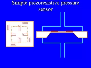
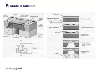
Pressure sensor. 2.008-spring-2003. Surface Micromachining. Pattern anchors. Deposit sacrificial layer. Deposit/pattern structural layer. Etch sacrificial layer. 2.008-spring-2003. Surface micromachining. Structure sacrificial etchant.

E N D
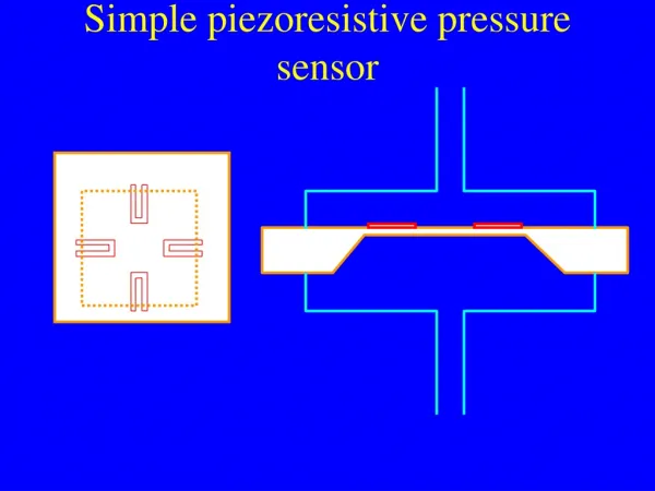
Pressure sensor 2.008-spring-2003
Surface Micromachining Pattern anchors Deposit sacrificial layer Deposit/pattern structural layer Etch sacrificial layer 2.008-spring-2003
Surface micromachining Structure sacrificial etchant Polysilicon Silicon dioxide HF SiNx PSG HF Silicon dioxide polysilicon XeF2 SiNx polysilicon XeF2 Aluminum photoresist oxygen plasma 2.008-spring-2003
Residual stress gradients More tensile on top More compressive on top Just right! 2.008-spring-2003
Clean Room Gowning with bunny suit Class 1, 10, 100 A salt grain on a chip 2.008-spring-2003
Class of clean rooms Class 1 means one speckle of 0.5 μ partical in one ft3. Class 10, 100, 1000 HEPA filter, AHU 2.008-spring-2003
Air Filters HEPA (High Efficiency Particulate Air) filters High efficiency, low Δp, good loading characteristics Glass fibers in a paper like medium 97% retainment of incident particles of 0.3 μm or larger 2.008-spring-2003
Class of clean rooms Class Temp tolerance tolerance 2.008-spring-2003
Particles Class Federal Standard 209; Number of particles per cubic foot 2.008-spring-2003
Toxicity TLV (Threshold Limit Value) Upper limit material concentration that an average healthy person can be exposed without adverse effects, ppm or mg/m3 Notorious Poisons CO (100 ppm), CO2 (5000 ppm), HCN (110 ppm), H2S (10 ppm) SO2 (5 ppm), NH3 (50 ppm) Arsenic trioxide AS2O3 (0.1g fatal) Hg (0.1 ppm via skin contact) All material are toxic in sufficient quantity, 5g caffein is fatal. 2.008-spring-2003
MEMS Applications 2.008-spring-2003
Display Technologies Market Leader Screen Size R.& D. Issues ●HDTV for 60” ~ 80” Home Theater ●Digital Presentation for 100 ” ~ 300” Projector ●Key Factor : Brightness 2.008-spring-2003
Brightness of Projection Displays lux = lumen / m2
PHOTONICS AND MICROMACHINING 1st Optical MEMS device DIGITAL MICROMIRROR DEVICE & DLP TM PROJECTOR CORPORATE RESEARCH & DEVELOPMENT 96365-39
DMD Optical Switching Principle DMD Mirror on/off ± 10o Texas Instruments’s Technical Journal: Vol. 15, No. 3, July-Sept. 1998. 2.008-spring-2003
DMD Cell Structure Texas Instruments’s Technical Journal: Vol. 15, No. 3, July-Sept. 1998. 2.008-spring-2003
TMA 2.008-spring-2003
Light Modulation of TMA Thinfilm Micromirror Array 2.008-spring-2003
Pixel Architecture Post contact to actuator Mirror Via contact to MOS Top Electrode PZT Bottom Electrode Supporting Layer Common Electrode Anchor Drain Pad Gate Line Source Line 2.008-spring-2003
TMA vs DMD TMATM (Daewoo Electronics) Piezoelectric DMDTM (Texas Instrument) Electrostatic Actuation 0o ~ 3o (continuous) -10o, 0o, +10o Tilting Angle Linear Simple On/Off Complex Gray Scale Control •Fatigue •Sticking •High Cost •Uniformity Drawbacks 2.008-spring-2003
Micromirror Arrays XGA 1024 X 768 786,432 pixels VGA 640 X 480 307,200 pixels 2.008-spring-2003
Mirror Flatness (VGA) 2.008-spring-2003
Coupled Natures of Thin Film Processes Forward coupling Step coverage, confromality Backward coupling Temperature dependent microstructural degradation Over/under etch, etch stop control Side attack, Passivation breakage 2.008-spring-2003
Evolution of TMA Pixels 2.008-spring-2003
MIT Bow-actuator Nick Conway, MS 2003 End effector Piezoelectric Amplifiers Released 4-bar linkage design Fixed substrate 2.008-spring-2003
Design of nanopipette (2): In-line array of nanopipettes Massive Parallel Nanopipette Array by In- plane Scanning Probe Systems Integration with Microfluidic channels Integration of nanopipettes in AFM in an 100 x 100 array Single nanopipette 2.008-spring-2003
Photonic crystal modeling Microcavity waveguide finite-difference time-domain 1 mesh 2.008-spring-2003
Photonic band gap microcavity waveguide processing design matrix of various geometries: defect lengths, waveguide width, d/a, number of holes Nanofabrication: SiNx mask1 /w electron-beam Proximity pattern transfer to resist 130 nm minimum features Hard mask from Cr lift-off 2 Optimized Si RIE 1 J. Ferrera, NanoStructures Laboratory, MIT. 2 J. Foresi, Kimerling group, MIT. 2.008-spring-2003
Design Domains Design is a mapping process From “What” to “How” Small scale systems design What How N. P. Suh, Axiomatic Design, Oxford 2.008-spring-2003