Download
1 / 6
60 likes | 201 Views
JEM Status and plans. RAL test results Hardware status Firmware Plans. RAL tests / Hardware status.

E N D
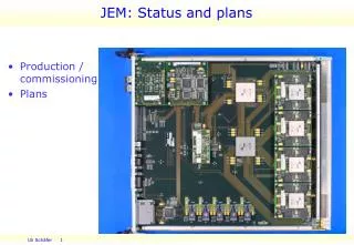
JEM Status and plans • RAL test results • Hardware status • Firmware • Plans
RAL tests / Hardware status … after a difficult start of last weeks tests, with software crashes, a probably TTC jitter related malfunction of the FPGAs, and a software problem mistaken for a firmware/hardware issue, we eventually succeeded operating both the jet and the energy algorithms, and we have successfully sent data to the mergers. Not so successful was a last-minute attempt to test the DAQ/ROI path. While the ROC spy memories tell us that the data presented to the G-links are correct and additional debug firmware confirmed that the DAV signal is asserted / deasserted as expected, the ROD would tell us that DAV is signaled where it shouldn't be. We are now increasingly concerned that the JEM G-links do not operate correctly due to excessive jitter on the clock. The risks have always been known and since we believe that we've seen even the FPGA DLLs lose lock with a JEM located far away from the TCM (this was never observed in the Mainz setup), problems with the G-links are only too probable. The situation is particularly bad on JEM0 due to * the use of old TTCrx chips * lack of a PLL clock distribution * the use of a clock mirror built from DLLs adding to the jitter * running the G-link STRBIN signal through the ROC internal clock distribution with yet another DLL All those issues will not be able to harm the operation of the JEM1 G-links since the clock mirror is now based on the new PLLed TTCdec and ordinary bus drivers which shouldn't add to the jitter. We will however, thoroughly test JEM0 with various measures to reduce jitter. If everything fails, we will operate the G-links off the local crystal clock, which unfortunately means that we can run either with constant data only, or we will have to live with the fact, that occasionally data packets will be corrupted due to the relative phase of transmitting to receiving module leading to setup violations on the receiving FPGA. After installation of new Cadence release, JEM1 design progressing well.
System ACE TTCdec CAN DES DAQ Input -- 10 X 9 W G Sum U To SMM 3 x 3 x 12 bit 40 Mb/s V M E DES Input 8 H 7 G 6 F 40 DAQ/Timing/VME T 60 To JMM DES Jet 5 E 4 D 3 C G 60 S ROI DES Input 2 B 1 A 0 V φ bins R 60 bit 80Mb/s each 165 pins FIO 88 pair JEM1 In input modules T,S probably mix of φ-bins 5,6 due to routing problems of high-speed LVDS links With current algorithm rounding errors will lead to dependency of the response on channel mapping… Modify algorithm
Algorithms (RTDP) Minor modifications to energy sum algorithm due to re-partitioning on JEM1: • Receive energies 4×8 ×(e/h) plus overlap (total 88 ch.) • Synchronisation, parity, mask • Generate jet elements ET=Ee+Eh , • Saturate jet elements at 1 TeV, send to jet processor @80Mb/s, 5-bit wide • From jet elements calculate EX and EY by multiplying cosφ, sinφ (accuracy: 10bit ET×12-bit coefficient -> 12-bit (.25 GeV resolution)) • Threshold (EX,EY), ET • Pre-sum EX, EY and ET : 12 jet elements (JEM0:4) • Truncate to 1GeV resolution • Saturate at 4 TeV • Send to sum processor @ 40Mb/s (JEM0:80Mb/s) : 12&14&14 bit • Final summation over 3 partial sums (JEM0:8) • Truncate to 1GeV resolution • Quad-linear encoding of energies (8 bit, 4 TeV range) • Saturation (4TeV) • Parity
H/W Status & Plans Plans: • Continue Mainz tests of energy and integrated (J/E) algorithms. • Joint tests w. Pre-Processor *now* • Jitter tests. • another RAL test in Dec ????? • ROD • Submit order for JEM1 component procurement along with assembly of remaining input daughters and JEM1 production *now* • Submit JEM1 main board design ~ end Dec., back from assembly Feb. • Set up stand-alone test bench for input processors after JEM1 submission (Andrey) to have well-tested daughter modules when JEM1 arrives • Keep JEM0s up and running through first stage of slice test
JEP – open questions • Slice data G-link format: do we change over to 6 input channels per G-link bit to allow for readout of 5 ticks worth of data at full rate? • No simple mapping of input channels to input processors in (η,φ) due to limitations on routing of high-speed tracks (length, vias). Do we sort it out in • Software (VME channel-address corresponds to location in the input processor), • Firmware (VME address corresponds to (η,φ)) , • Re-format slice data in ROC ? • Sum CMM : stay with LUT scheme or change to EX*EX+EY*EY >=threshold*threshold (might cost ~1 tick latency)