Download
1 / 29
310 likes | 472 Views
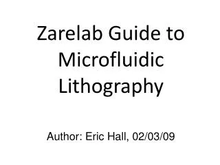
Zarelab Guide to Microfluidic Lithography. Author: Eric Hall, 02/03/09. Introduction. The process through which we make microfluidic chips is called lithography . This presentation is an introduction to how we do lithography in the Zarelab.

E N D
Zarelab Guide to Microfluidic Lithography Author: Eric Hall, 02/03/09
Introduction • The process through which we make microfluidic chips is called lithography. This presentation is an introduction to how we do lithography in the Zarelab. • There are actually two types of lithography involved in making a microfluidic chip: • Photolithography: Making a mold on a silicon wafer using UV light to etch a design • Soft lithography: Using the mold to make a chip from polydimethyl siloxane (PDMS) polymer
Sample Chip Design We start with a chip design. Below is a simple sample design that we’ll be using as an example. Top View 70µm x 7µm Channel 70µm x 1µm Channel Peristaltic Pump Side View Hole-Punched Inlet
Part I: Photolithography
Photolithography • The purpose of photolithography is to create small structures or features on a silicon wafer using photoresist. Features are made out of photoresist by etching with UV light. • Photolithography uses this general process: • Wafer priming • Spincoating • Prebaking • Exposure • Development • Postbaking (varies depending on resist type)
Photoresist • There are two types of photoresist: • Positive: Exposure to UV light removes resist • Negative: Exposure to UV light maintains resist Mask Positive Resist Negative Resist
Masks Prior to doing photolithography, we need to make exposure masks for our mold. These are used during the exposure step of photolithography to etch the desired design into the photoresist. 70 µm x 7 µm Channel 70 µm x 1 µm Channel The channel mold has two different feature thicknesses: 7 µm and 1 µm. Therefore, we need two separate masks for the two different resist layers.
Masks Mask for 7µm-thick Positive Resist Layer Mask for 1µm-thick Negative Resist Layer The crosses are alignment marks. They are used to align the mask for the second layer to the features of the first layer.
Negative Resist Photolithography We’ve made two masks because the wafer has two feature layers: a 7 µm positive resist layer and a 1 µm negative resist layer. Question: Why do we first make the negative resist layer? Answer: Exposing the negative resist to light a second time (during the positive resist exposure) does nothing. Exposing the positive resist to light (during the negative resist exposure) would further etch it.
Negative Resist Photolithography Step 1: Wafer Priming All wafers need to be primed with HMDS to increase adhesion of the photoresist to the wafer. This can be done either in the yes oven or svgcoat track. Step 2: Spincoating The wafer is placed on a rotating platform, or “chuck”, and held via vacuum suction. Resist is poured onto the wafer. The wafer spins at high speed (several thousand rpm’s). The speed determines the resist thickness.
Negative Resist Photolithography Step 2: Spincoating (cont.) For negative resist, we use SU-8. It comes in various concentrations for different resist thickness ranges. Please refer to www.microchem.com for more info. We use the headway2 instrument for negative resist. 2 – 4 krpm Step 3: Prebaking Following spincoating, wafers need to be baked on a hotplate. Refer to the SU-8 data sheets at www.microchem.com.
Negative Resist Photolithography Step 4: Exposure Wafers are exposed to UV light using the karlsuss or evalign instruments. A mask is used to transfer the design to etch the design onto the spincoated resist. The energy and time required can vary with resist thickness, so refer to the SU-8 data sheets.
Negative Resist Photolithography Step 5: Postbaking Following exposure, wafers need to be baked on a hotplate again. Refer to the SU-8 data sheets for baking times. Step 6: Development Wafers are placed in SU-8 developer, which removes resist that was not exposed to UV light. Only the desired features remain. Development times vary with thickness, so refer to the SU-8 data sheets.
Positive Resist Photolithography For all subsequent layers after the first layer, do NOT re-prime the wafer. Wafers with photoresist on them cannot be put in priming instruments. Step 1: Spincoating & Prebaking For positive resist (SPR 220), we use the svgcoat instruments. These are automated tracks where pre-set recipes are used for specific thicknesses. Different thicknesses require different prebaking strategies. Ask a section member for advice.
Positive Resist Photolithography Step 2: Exposure Once again, the karlsuss or evalign instruments are used for exposure. There are no reliable data sheets for SPR resist. Therefore, ask a section member for advice on what settings to try first. Step 3: Development Use the automated svgdev tracks for positive resist.
Positive Resist Photolithography Step 4: Postbaking (optional) If your positive resist is a mold for a channel that will have a valve or pump above it (like in this sample design), you should postbake it. This curves the cross-section, which allows for complete closure of the channel. Postbaking should be done at 120 oC for at least 5 min. Check the profile using a microscope. If no valve is employed, there is no need to postbake. Postbaking 120 oC, 5 min
Final Tips for Photolithography • Before taking your wafers out of the SNF, check them under a microscope to make sure that the features came out the way you wanted. • When you get back to the Zarelab, place the wafers in a dessicator under silanes for a half hour. This protects the photoresist from the degradation that comes from continued use. • Be prepared to make multiple wafers. Normally, a few will serve to test parameters such as exposure time, as instrument parts like the UV lamp can change intensity and uniformity over time.
Part II: Soft Lithography
Soft Lithography The molds we created using photolithography in the SNF can now be used to create microfluidic chips via soft lithography. Unlike photolithography, soft lithography can be conducted in our Bio-X lab. There are a wide variety of soft lithography techniques. This part of the presentation will simply guide you through lithography of a very simple chip using basic techniques. If you encounter any soft lithography challenges or questions, ask the other section members. They will have more than a few ideas of how to proceed.
Lithography in Layers Pump Layer Channel Layer Side View Hole-Punched Inlet Soft lithography is done in layers. In this chip, there are two: the ‘pump’ layer and the ‘channel’ layer. Each is made from a mold. We made the channel layer mold in the previous photolithography section. Assume that we’ve also made the pump layer mold.
Pump Layer Step 1: Pump Layer Mix 10:1 PDMS A:B and pour over the mold for the pump layer. Place in the vacuum dessicator to remove all gas bubbles. Completely cure at 80oC.
Pump Layer Step 1: Pump Layer (cont.) Cut pump layer from the wafer. Using gloves and a hole punch, create inlets for the three pump valves.
Channel Layer Step 2: Channel Layer Mix 10:1 PDMS A:B and pour over the mold for the channel layer. Spincoat PDMS on the wafer at the appropriate speed for the desired thickness. Partially cure at 80oC.
Channel Layer Step 2: Channel Layer (cont.) Align the pump layer and press down onto the channel layer. Completely cure the joined layers at 80oC.
Channel Layer Step 2: Channel Layer (cont.) Cut the pump-channel chip from the wafer. Using gloves and a hole punch, create inlets for the two ends of the channel.
Coverslip Step 3: Glass Coverslip Mix 10:1 PDMS in cyclohexane in a 1:2 mass ratio. Pour onto class goverslip. Spincoat PDMS/cyclohexane on the wafer at the appropriate speed for the desired thickness. The cyclohexane allows for a thinner layer. Partially cure at 80oC.
Coverslip Step 3: Glass Coverslip (cont.) Partially cure at 80oC. Partial curing requires removing the PDMS from the oven prior to cross-linking completion. The PDMS is still molten, though the degree can be greatly varied by the curing time. More molten PDMS can more strongly bond to a substrate, but it is also more susceptible to ‘filling in’ open structures (e.g. channels) and being distorted.
Coverslip Step 3: Glass Coverslip (cont.) Place the pump-channel chip onto the PDMS-coated glass coverslip. Completely cure the complete chip at 80oC. It is recommended that the final cure be done overnight to ensure complete bonding.
Conclusion This concludes the introductory guide to microfluidic lithography. Now that you have seen the process of making a chip, you should better understand the considerations that go into making a design. Remember though that this is simply an introduction. Chip design and lithography are complex, nuanced subjects. Please shadow your fellow section members before doing your first lithography run. Also, when making a design, please ask them for input and advice.