Download

1 / 49
550 likes | 838 Views
Verilog Fundamentals. Shubham Singh Junior Undergrad. Electrical Engineering. VERILOG FUNDAMENTALS. HDLs HISTORY HOW FPGA & VERILOG ARE RELATED CODING IN VERILOG. HDLs HISTORY . HDL – HARDWARE DESCRIPTION LANGUAGE. EARLIER DESIGNERS USED BREADBOARDS FOR DESIGNING. SOLDERLESS BREADBOARD.

E N D
Verilog Fundamentals Shubham Singh Junior Undergrad. Electrical Engineering
VERILOG FUNDAMENTALS • HDLs HISTORY • HOW FPGA & VERILOG ARE RELATED • CODING IN VERILOG
HDLs HISTORY HDL – HARDWARE DESCRIPTION LANGUAGE
EARLIER DESIGNERS USED BREADBOARDS FOR DESIGNING SOLDERLESS BREADBOARD PRINTED CIRCUIT BOARD
HDLs ENABLED LOGIC LEVEL SIMULATION AND TESTING GATE LEVEL DESCRIPTION SIMULATE MANUAL
THEN DESIGNERS BEGAN TO USE HDLs FOR HIGHER LEVEL DESIGN BEHAVIOURAL ALGORITHM SIMUALTE MANUAL SIMULATE REGISTER TRANSFER LEVEL MANUAL SIMULATE GATE LEVEL MANUAL
HDLs LED TO TOOLS FOR AUTOMATIC TRANSLATION SIMULATE BEHAVIOURAL ALGORITHM MANUAL SIMULATE REGISTER TRANSFER LEVEL LOGIC SYNTHESIS SIMULATE GATE LEVEL AUTOPLACE & ROUTE
THE CURRENT SITUATION C,C++ MATLAB BEHAVIOURAL VERILOG COMPILERS ARE NOT AVAILABLE TO CONVERT BEHAVIOURAL LEVEL TO REGISTER TRANSFER LEVEL STRUCTURAL VERILOG LOGIC SYNTHESIS GATE LEVEL
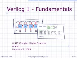
MUX 4 : GATE LEVEL DESIGNING modulemux4(input a,b,c,d, input[1:0] sel, output out); wire[1:0] sel_b; not not0( sel_b[0], sel[0] ); not not1( sel_b[1], sel[1] ); wire n0, n1, n2, n3; and and0( n0, c, sel[1] ); and and1( n1, a, sel_b[1] ); and and2( n2, d, sel[1] ); and and3( n3, b, sel_b[1] ); wirex0, x1; nor nor0( x0, n0, n1 ); nor nor1( x1, n2, n3 ); wirey0, y1; or or0( y0, x0, sel[0] ); or or1( y1, x1, sel_b[0] ); nand nand0( out, y0, y1 ); endmodule
MUX 4 : REGISTER TRANSFER LEVEL Module mux4( input a, b, c, d input[1:0] sel, Output out ); wire out, t0, t1; assign out = ( sel == 0 ) ? a : ( sel == 1 ) ? b : ( sel == 2 ) ? c : ( sel == 3 ) ? d : 1’bx; endmodule
VERILOG • Verilog is a HARDWARE DESCRIPTION LANGUAGE. • HDLs are used to describe a digital system • Not a programming language despite the syntax being similar to C • Synthesized (analogous to compiled for C) to give the circuit logic diagram
FPGAs • Field Programmable Gate Array • A Fully configurable IC • FPGAs contain programmable logic components called logic blocks. • Contain hierarchy of reconfigurable interconnects that allow the blocks to be wired together. • Logic Blocks can be configured to any complex circuit. • FPGA can be made to work as a Xor gate, a Counter or even bigger- an entire Processor!
HOW TO PROGRAM FPGAs • Configured using a Hardware Description Language • Can be configured by any way by the user • Basic Idea : VERILOG SYNTHESISER BEHAVIOURAL DESCRIPTION OF REQUIRED CIRCUIT A COMPLETE CIRCUIT DIAGRAM
CODING IN VERILOG • BREAKING CIRCUITS INTO VARIOUS BUILDING BLOCKS CALLED “MODULE” • DEFINING MODULE • CONNECTING VARIOUS MODULES
CODING IN VERILOG • Communication between a module and its environmentis achieved by using Ports • Ports are of three types: input, output, inout
AN EXAMPLE : 4029 COUNTER • • Name: 4029 • • Input Ports: One • • Output Ports: Four • Size • Driver type • • Internal Logic: At every rising edge of the clock, increment the output by one
MODULE • A “Black Box” in Verilog with inputs, outputs and internal logic working. • So, a module can be used to implement a counter. • A module is defined as module <specific type>(<port list>);
DEFINING 4029 MODULE • Way 1: module 4029(clk,out,reset,enable); • Way 2: module 4029(clk, a, b, c, d, reset, enable); • Input and Output Ports in each of the above? • EVERY PORT MUST HAVE A DIRECTION AND BITWIDTH • Every module ends with the statement endmodule
DECLARING PORTS • Way 1: input clk; input reset; input enable; output a,b,c,d; • Way 2: input clk; input reset; input enable; output [3:0] out;
DRIVERS IN VERILOG • We need drivers for this module in order to interact with the ports and describe its logical working. • Two types of drivers: • Can store a value (for example, flip-flop) : REG • Cannot store a value, but connects two points (for example, a wire) : WIRE
DRIVERS IN 4029 • Ports defined as wires? • clk • reset • enable We do not need to stores the values of these ports in our logical block. • Ports defined as reg? • a,b,c,d • out We need to store them so that we could modify their values when required.
DEFINING DRIVERS FOR 4029 • Way 1: wire clk; wire reset; wire enable; rega,b.c,d; • Way 2: wire clk; wire reset; wire enable; reg [3:0] out;
OPERATORS AND CONDITIONAL OPERATORS • All the arithmetic as well as logical operators in Verilog are similar to C, except ++ and --which are not available in Verilog. • Conditional statements are also similar to C with following modifications: • { is replaced by begin. • } is replaced by end.
COMBINATIONAL CIRCUITS • Combinational circuits are acyclic interconnections of gates. And, Or, Not, Xor, Nand, Nor …… Multiplexers, Decoders, Encoders …. • OUTPUT IS A FUNCTION OF PRESENT INPUT ONLY
How are these gates, muxs etc. abstracted in Verilog? Gates, Add, Multiply … : by simple operators like in C Multiplexers … : by control statements like if-else, case, etc Gate level implementation of above high level operators done by Verilog synthesizer.
SEQUENTIAL CIRCUITS • Circuits containing state elements are called sequential circuits • OUTPUT DEPENDS ON THE PRESENT INPUT AS WELL AS ON ITS PRESENT STATE. • How do you implement such an element in Verilog?
always block • Syntax always @(condition) begin //Code end • Blocks starting with keyword always run simultaneously. • @ symbol is used to specify the condition which should be satisfied for the execution of this block.
Usage of always block • always The code in this block will keep on executing. • always @(a) The code in this block will be executed every time the value of a changes. • always @(posedge clk) This block is executed at every positive edge of clk.
always @ BLOCK • It is an abstraction provided in Verilog to mainly implement sequential circuits. • Also used for combinational circuits.
BLOCKING AND NON-BLOCKING ASSIGNMENTS • Non-blocking assignments happen in parallel. always @ ( #sensitivity list # ) begin B <= A ; C <= B ; (A,B) = (1,2) -> (B,C) = (1,2) end • Blocking assignments happen sequentially. always @ ( #sensitivity list # ) begin B = A ; C = B ; (A,B) = (1,2) -> (B,C) = (1,1) end
POINTS TO NOTE • Use always@(*) block with blocking assignments for combinational circuits • Use always@( posedgeCLK) block with non-blocking assignments for sequential circuits. • Do not mix blocking and non-blocking assignments.
A COMPLETE 4029 MODULE module 4029 ( input wire clk, input wire reset, input wire enable, output [3:0] reg out); //You can declare direction as well as data type //in the module definition.
always @(posedge clk) begin if (reset == 0 && enable == 0) begin out <= out +1; end end
always @(reset or enable) begin if (reset == 1’b1) begin out <= 0; end end endmodule
Various modules are interconnected to make a larger circuit (or module). Each sub-module has a separate Verilog file. A sub-module may have another sub-module in its circuit. One needs to indicate the top level module before synthesis.
EXAMPLE • module 4029(input wire clk, output [3:0]reg out); • module 7447(input [3:0] reg in, output [6:0] reg bcd); • module TOP(input wire clk, output [6:0] reg bcd);
INSTANTIATION • USED TO INTERCONNECT VARIOUS MODULES • In the above example, we need to instantiate the two sub-modules in the top level module • THIS IS DONE AS FOLLOWS: wire [3:0] c; 4029 counter (.clk(clk), .out(c) ); 7447 decoder (.in(c), .bcd(bcd));
Problem Statement • Level 1 : Theoretical Questions on basic syntax of Verilog • Level 2 : Design a digital system using Verilog . (weightage will be given to how much modular your circuit is )