Chapter6 Combinational Logic Design Practices
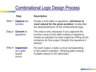
Chapter6 Combinational Logic Design Practices. — Comparator — Adder. EN SEL D0 Dn-1. Enable ( 使能 ). Select ( 选择 ). EN SEL D0 Dn-1. Data Output ( 数据输出 ) ( b 位). Y. N Data Sources (n 个 b 位数据源 ). n 个1位数据源. Y. Multiplexer. Enable 使能. Select 选择. 数据输出(1位). SRCA. DSTA.

Chapter6 Combinational Logic Design Practices
E N D
Presentation Transcript
Chapter6 Combinational Logic Design Practices — Comparator —Adder
EN SEL D0 Dn-1 Enable (使能) Select (选择) EN SEL D0 Dn-1 Data Output (数据输出)(b位) Y N Data Sources (n个b位数据源) n个1位数据源 Y Multiplexer Enable 使能 Select 选择 数据输出(1位)
SRCA DSTA SRCB DSTB BUS 多路 分配器 多路 复用器 SRCZ DSTZ SRCSEL DSTSEL SRC : source SEL : select DST : destination Demultiplexer (多路分配器) • Route the bus data to one of m destinations (把输入数据送到m个目的地之一)
1 变量为1的个数是奇数 1 变量为1的个数是奇数 X0 X1 … Xn = A0 A1 … An = 0 变量为1的个数是偶数 0 变量为1的个数是偶数 Parity Circuit(奇偶校验电路) • Odd-Parity Circuit(奇校验电路) • Output is 1 if an odd number of its inputs are 1. • Even-Parity Circuit(偶校验电路) • Output is 1 if an even number of its inputs are 1.
6.9 Comparator (比较器) • Comparing two binary words is a common operation in computers. • Comparator: Check if two Binary words are equal ( 等值比较器) • Magnitude Comparator: Compare their magnitude (Greater than, Equal, Less than) (数值比较器)
A B EQ A B DIFF DIFF : different EQ : equal Comparator • How to build a 1-bit Comparator? ——Use XOR (XNOR)
——并行比较 ——串行比较 A0 B0 必须每位都相等 A1 B1 DIFF A2 B2 4-bit comparator A3 B3 How to Build a N-bit Comparator? The DIFF output is asserted if any of the input-bit pairs are different. This circuit can be easily adapted to any number of bits per word.
Primary inputs PI0 PI1 PIn-1 C0 PI CI CO PO C1 PI CI CO PO C2 PI CI CO PO Cn PO0 PO1 POn-1 Primary outputs Iterative circuit(迭代电路) Iterative:重复的, 反复的, [数]迭代的 Boundary inputs Boundary outputs Cascading output
A B EQ Cascading input EQO EQI X0 Y0 X1 Y1 XN-1 YN-1 X Y CMP EQI EQO X Y CMP EQI EQO X Y CMP EQI EQO EQ1 EQ2 EQN-1 EQN An Iterative Comparator —— 每位串行比较 1 迭代的方法可能节省费用,但速度慢 Figure 6-77
(A’·B)’ A LT_L EQ_L GT_L B (A·B’)’ 1-Bit Magnitude Comparator (一位数值比较器) ① A>B(A=1, B=0)则 A·B’=1 可作为输出信号 ② A<B(A=0, B=1)则 A’·B=1 可作为输出信号 ③ A=B ,则A⊙B=1,可作为输出信号 输出低电平有效 LT : Less Than EQ : Equal GT : Greater Than EQ_L = A·B’+A’·B = AB = (A⊙B)’
A3·B3’ + ⊙ A2·B2’ + ⊙ ⊙ A1·B1’ + ⊙ ⊙ ⊙ A0·B0’ n-Bit Magnitude Comparator(多位数值比较器) A(A3A2A1A0)和B(B3B2B1B0)自高而低逐位比较 EQ = (A3⊙B3)·(A2⊙B2)·(A1⊙B1)·(A0⊙B0) GT = (A3>B3) 或 (A3 =B3)·(A2>B2) 或 (A3 =B3)· (A2 =B2)·(A1>B1) 或 (A3 =B3)·(A2 =B2)·(A1 =B1)·(A0>B0) LT = EQ’ · GT’ = ( EQ + GT )’
级联输入,用于扩展 74x85 ALTBIN AEQBIN AGTBIN A=B:低位和高位都相等 A0 A1 A2 A高位>B高位 A高位=B高位 & A低位>B低位 A>B A3 ALTBOUT = (A<B) + (A=B)·ALTBIN 4-Bit Comparator 74x85 ( 4位比较器74x85) 通常低位的输出接高位的输入 AEQBOUT = (A=B)·AEQBIN AGTBOUT = (A>B) + (A=B)·AGTBIN
低位 高位 +5V 74x85 74x85 74x85 A<BO A=BO A>BO A<BO A=BO A>BO A<BO A=BO A>BO A<BI A=BI A>BI A<BI A=BI A>BI A<BI A=BI A>BI [7:4] [3:0] [11:8] A0~A3 A0~A3 A0~A3 B0~B3 B0~B3 B0~B3 XD[11:0] YD[11:0] Serial Expanding Comparators(比较器的串行扩展) 3片74x85构成12位比较器 X<Y X=Y X>Y
P0 P1 P2 P3 GE P4 P5 LT P6 P7 8-bit comparator 74x682 P464 Figure 6-82 问题1:怎样表示以下输出? • active-high:P DIFF Q • active-high :P EQ Q • active-high :P GE Q • active-high :P LT Q (P463 图6-81) 问题2:能否扩展?? 注意:没有级联输入端
Q[23:0] P[23:0] P0~P7 P=Q Q0~Q7 P>Q [7:0] PEQQ P0~P7 P=Q Q0~Q7 P>Q [15:8] PGTQ P0~P7 P=Q Q0~Q7 P>Q [23:16] Parallel Expanding Comparators(比较器的并行扩展) 3片74x682构成24位比较器
Applications of comparator ——对产品分装的方框图 产品在传送带上输送,经过光电变换,将获得的与产品个数一致的电脉冲放大整形,加到计数器上计数。 当计数器计得的数目与设定值相等时,比较器输出高电平,用这个高电平去控制相应的装置,使产品分箱。
(半加器真值表) A B CO S 0 0 0 0 0 1 0 1 1 0 0 1 1 1 1 0 6.10 Adder (加法器) Half Adder andFull Adder(半加器和全加器) Sum (相加的和): S = A’·B + A·B’ = A B Carry (向高位的进位): CO = A·B Truth Table of Half Adder 0 1 0 1 +0+0+1+1 0 1 1 10 it is only “Half” because it doesn’t consider a “Carry In” bit
CO XY 全加器真值表 00 01 11 10 CI CI X Y CO S 0 0 1 0 Truth Table of Full Adder 0 0 0 0 0 0 0 0 1 0 1 0 1 0 0 1 0 1 1 1 0 1 0 0 0 1 1 0 1 1 0 1 1 0 1 0 1 1 1 1 1 0 1 1 1 1 X Y CI S CO Adder Half Adder andFull Adder(半加器和全加器) to create a full adder, we need to include the “Carry In” in the Sum CO =++ Y·CI X·CI X·Y = X·Y + (X+Y)·CI S = X Y CI
X0 Y0 X1 Y1 X2 Y2 X3 Y3 X Y CI CO S X Y CI CO S X Y CI CO S X Y CI CO S C1 C2 C3 C4 C0 S0 S1 S2 S3 Ripple Adder (串行进位加法器) • A ripple adder is a cascade of n full-adders stages, each of which handles one bit. =0 tADD = tXYCout + (n-2)*tCinCout + tCinS Disadvantage: Slow, More Propagation Delay —— Improve Speed: Parallel Adder 回顾:串行比较器
An Iterative Comparator X0 Y0 X1 Y1 XN-1 YN-1 X Y CMP EQI EQO X Y CMP EQI EQO X Y CMP EQI EQO EQ1 EQ2 EQN-1 EQN 1 X0 Y0 X1 Y1 X2 Y2 X3 Y3 Primary Inputs X Y CI CO S X Y CI CO S X Y CI CO S X Y CI CO S C1 C2 C3 C4 C0 S0 S1 S2 S3 级联输出 Primary Outputs Ripple Adder Boundary Outputs Boundary Inputs
全加器真值表 Ci X Y Ci+1 S 一位全加器:S = X Y Ci 0 0 0 0 0 0 0 1 0 1 0 1 0 0 1 0 1 1 1 0 1 0 0 0 1 1 0 1 1 0 1 1 0 1 0 1 1 1 1 1 Ci+1 = X·Y + (X+Y)·Ci Carry generate 进位产生信号 Carry propagate 进位传递信号 Carry-Lookahead Adder(先行进位加法器) Carry lookahead (先行进位法):第 i位的进位输入信号可以由该位以前的各位状态决定。 Ci+1 = (Xi·Yi) + (Xi+Yi)·Ci = Gi+ Pi· Ci
S3 S2 S1 S0 ∑ CI CO 74LS283 A3 A1 B3 B1 A2 A0 B2 B0 Carry-Lookahead Adder 先行进位法:第 i位的进位输入信号可以由该位以前的各位状态决定。 Ci+1 = Gi + Pi· Ci C0 = 0 MSI加法器 74x283 P480 图6-87 C0 = 0 C1 = G0+P0·C0 C2 = G1+P1·C1 = G1+P1·(G0+P0·C0) = G1+P1·G0+ P1·P0·C0 … … Cn = Gn+Pn·Cn 展开为“与-或”式:三级延迟
74x181 G P S0~S3 M A=B CIN F0~F3 A0~A3 输入数据 B0~B3 COUT MSI Arithmetic and Logic Units (ALU, MSI 算术逻辑单元) • Perform any of a number of different arithmetic and logical operations on a pair of b-bit operands. 选择特定操作 0算术/1逻辑 输出数据 Table 6-70
S3 S2 S1 S0 ∑ CI CO 74LS283 A3 A1 B3 B1 A2 A0 B2 B0 加法器应用举例 1. 用四位二进制加法器74x283实现8421BCD码与余3码的转换 解:设 8421BCD码A=A3A2A1A0 余3码Y=Y3Y2Y1Y0 8421BCD码 ----?---> 余3码 ----->给定数值的余3码总比8421BCD码多3 Y3Y2Y1Y0=A3A2A1A0+0011
余3码 Y3 Y2 Y1 Y0 ∑ 0 CI CO 74LS283 A3 A1 B3 B1 A2 A0 B2 B0 A3 A2 A1 A0 0 0 1 1 8421BCD码 8421BCD码 ----> 余3码 思考?如何将余3码----?--->8421BCD码
加法器应用举例 2. 用四位二进制加法器74x283设计四位二进制加法/减法器 解:要实现加法和减法双重功能,需要有功能选择信号,用M表示。 • 设A=A3A2A1A0为四位二进制被加数(或被减数),B=B3B2B1B0为四位二进制加数(或减数)。 • 当M=0时,电路实现A+B的加法运算 • 当M=1时,电路实现A-B的减法运算。
减法运算用补码实现 所以有 即将减法运算变成了加法运算,但减数B的各位应该为原数值位的非 考虑到异或门的特性 所以通过四位加法器和异或门可以实现加法器/减法器
Summary • Documentation Standards and Circuit Timing • Decoders 、Encoders 、Multiplexers 、Parity Circuits 、Comparators 、Adders • Definition/Function… • Standard MSI… • Expanding/cascading… • Build logic function…
功能表 S1 S0 Y 0 0 0 1 1 0 1 1 A·B A+B AB A’ 真值表 S1 S0 A B Y 0 0 0 0 0 0 0 1 Ex. 设计函数发生器,其功能表如下: 1、填写真值表 2、选择器件 • 用基本门电路实现 利用卡诺图化简 • 用译码器实现 转换为最小项之和 • 用数据选择器实现 3、电路处理 注意有效电平
Homework • 6.29 • 6.38 • 6.43 • 6.51 • 6.52 • 6.53 思考: • 6.31* 6.39* 6.77*