Comprehensive Guide to Combinational Logic Circuit Design
This guide outlines the design procedure for combinational logic circuits, emphasizing key steps such as specification, formulation, optimization, and technology mapping. It explores mapping Boolean inputs to outputs through various logic gates (AND, OR, NOT, NAND, NOR) and highlights the importance of hierarchical design to manage complexity. By decomposing functions into smaller blocks, designers can efficiently create complex systems. It also discusses verification techniques, ensuring the correctness of the final design through both manual methods and simulation.

Comprehensive Guide to Combinational Logic Circuit Design
E N D
Presentation Transcript
Combinatorial Logic Circuit m Boolean Inputs n Boolean Outputs Combinational Circuits • A combinational logic circuit has: • A set of m Boolean inputs, • A set of n Boolean outputs • n switching functions, each mapping the 2m input combinations to an output such that the current output depends only on the current input values A block diagram
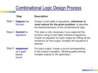
Design Procedure Steps • Specification • Formulation • Optimization • Technology Mapping: • AND, OR, and NOT; NAND; NOR • Verification • Manual • Simulation
Design Procedure • Specification • Write a specification for the circuit if one is not already available • Formulation • Derive a truth table or initial Boolean equations that define the required relationships between the inputs and outputs, if not in the specification • Apply hierarchical design if appropriate (more later)
Design Procedure • Optimization • Apply 2-level and multiple-level optimization • Draw a logic diagram (or provide a netlist ) for the resulting circuit using ANDs, ORs, and inverters
Design Procedure • Technology Mapping • Map the logic diagram or netlist to the implementation technology selected • Verification • Verify the correctness of the final design manually or using simulation
Hierarchical Design • Objective: To control the complexity of each function which is mapping inputs to outputs • Decompose the function into smaller pieces called blocks • Decompose each block’s function into smaller blocks, repeating as necessary until all blocks are small enough • Any block not decomposed is called a primitive block • The collection of all blocks including the decomposed ones is a hierarchy
Design Hierarchy • Just like with a large software program, to design a large chip you need a hierarchy • Divide and Conquer • Block is equivalent to object
Example: 9-input even parity checker • Design a 9-input function to check even parity for byte • Chapter 2: Use odd function circuit to check even parity
We know how to design an XOR Y X • A NAND only implementation is: X Y
The blocks that must be designed Components in Design
9-input parity tree (continued) • Top Level: 9 inputs, one output • 2nd Level: Four 3-bit odd funcions in two levels • 3rd Level: Two 2-bit exclusive-OR functions • Primitive block, XOR gate: Four 2-input NAND gates • Design requires {4 X (2 X 4)} = 32 2-input NAND gates
Top Down Design • Ideally you specify top level of design and work your way down • Real life isn’t that way • Work some at top • Build/test some low-level blocks • Go back to top level • Just like real software programs • Big projects (like Pentium) done with architecture and levels of simulators