Download
1 / 25
250 likes | 267 Views
An incremental position sensor with on-chip encoding for direct digital output is the TRACKER NSE-5310. An external magnetic strip is mounted above the IC at a distance of 0.3 mm (typ), and its incremental location is determined using a Hall element array on the chip.<br><br>This sensor array locates the magnetic strip's endpoints to serve as a zero reference.<br>

E N D
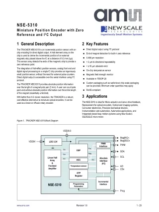
NSE-5310 Miniature Position Encoder with Zero Reference and I²C Output 1 General Description 2 Key Features Direct digital output using I²C protocol The TRACKER NSE-5310 is an incremental position sensor with on- chip encoding for direct digital output. A Hall element array on the chip is used to derive the incremental position of an external magnetic strip placed above the IC at a distance of 0.3 mm (typ). This sensor array detects the ends of the magnetic strip to provide a zero reference point. End-of-magnet detection for built-in zero reference 0.488 μm resolution < 2 μm bi-directional repeatability < ±10 µm absolute error The integration of Hall-effect position sensors, analog front end and digital signal processing on a single IC chip provides an ingeniously small position sensor, without the need for external pulse counters. Direct digital output is accessible over the serial interface using I²C protocol. On-chip temperature sensor Magnetic field strength monitor Available in TSSOP-20 Custom packaging such as wafer-level chip scale packaging can be provided. Minimum order quantities may apply. The TRACKER NSE-5310 provides absolute position information over the length of a magnet pole pair (2 mm). A user can count pole pairs and achieve absolute position information over the entire length of the magnet (essentially unlimited). RoHS compliant 3 Applications With better than 0.5 micron resolution, the TRACKER is a robust, cost-effective alternative to miniature optical encoders. It can be used as a linear or off-axis rotary encoder. The NSE-5310 is ideal for Micro-actuator and servo drive feedback, Replacement for optical encoders, Optical and imaging systems, Consumer electronics, Precision biomedical devices, Instrumentation and automation, Automotive applications, and Integrated closed-loop motion systems using New Scale’s SQUIGGLE micro motor. Figure 1. TRACKER NSE-5310 Block Diagram VDD3V3 MagINCn MagDECn VDD5V LDO 3.3V PWM Interface PWM Pos Sin DSP SDA Mag Cos SCL Linear Hall Array & Frontend Amplifier Absolute Interface (I2C) AGC AGC AGC AO CSn Temperature sensor OTP Register Incremental Interface NSE-5310 Programming Parameters Prog www.ams.com Revision 1.6 1 - 25
NSE-5310 Datasheet - Applications Contents 1 General Description.................................................................................................................................................................. 2 Key Features............................................................................................................................................................................. 3 Applications............................................................................................................................................................................... 4 Pin Assignments....................................................................................................................................................................... 1 1 1 3 4.1 Pin Descriptions.................................................................................................................................................................................... 5 Absolute Maximum Ratings...................................................................................................................................................... 6 Electrical Characteristics........................................................................................................................................................... 3 5 6 6.1 Magnet Input Specification................................................................................................................................................................... 6.2 Electrical System Specifications........................................................................................................................................................... 6.3 DC/AC Characteristics for Digital Inputs and Outputs.......................................................................................................................... 7 Detailed Description.................................................................................................................................................................. 6 7 8 9 7.1 Using 3.3V or 5V Operation................................................................................................................................................................ 8 Application Information........................................................................................................................................................... 11 12 8.1 Hall Sensor Array ............................................................................................................................................................................... 8.2 Automatic Gain Control (AGC)........................................................................................................................................................... 8.3 Temperature Sensor........................................................................................................................................................................... 8.4 I²C User Interface............................................................................................................................................................................... 8.4.1 Sync Mode................................................................................................................................................................................. 14 8.5 Z-axis Range Indication (“Red/Yellow/Green” Indicator).................................................................................................................... 8.6 Pulse Width Modulation (PWM) Output.............................................................................................................................................. 8.7 Magnetic Strip Requirements............................................................................................................................................................. 8.7.1 Mounting the Magnet................................................................................................................................................................. 16 8.8 Programming the NSE5310................................................................................................................................................................ 8.8.1 Zero Position Programming....................................................................................................................................................... 18 8.8.2 User Selectable Settings ........................................................................................................................................................... 19 8.9 Fast / Slow Mode:............................................................................................................................................................................... 9 Package Drawings and Markings........................................................................................................................................... 12 12 12 13 15 15 16 18 20 21 9.1 Recommended PCB Footprint............................................................................................................................................................ 10 Ordering Information............................................................................................................................................................. 22 24 www.ams.com Revision 1.6 2 - 25
NSE-5310 Datasheet - Pin Assignments 4 Pin Assignments Figure 2. Pin Assignments (Top View) NC NC 1 20 MagIncrn VDD5V 2 19 MagDecrn VDD3V3 3 18 4 NC DTest1_A 17 NC DTest2_B 5 16 NSE-5310 PWM 6 15 TestCoil CSn Mode_Index 7 14 SCL / CLK VSS 8 13 SDA / DIO 12 PDIO 9 I2C_A0 NC 11 10 4.1 Pin Descriptions Table 1. Pin Descriptions Pin Number Pin Name Pin Type Description Not Connected 1 NC 2 MagINCn Indicates Increasing or Decreasing of Magnitude by the AGC. Both signals are active low if AGC is in Non Valid Range. 3 MagDECn Digital output open drain Test output in default mode, A in sync mode 4 DTEST1_A Test output in default mode, B in sync mode 5 DTEST2_B Serial connection of Hall Element Coils to VSS 6 Coil Analog I/O Decimation Rate Selection internal pull down, by default DCR = 256. Static setup at power up. Digital I/O with pull-down Digital output open drain 7 Mode_Index Ground 8 VSS Supply pad Digital I/O Analog I/O Digital and Analog Access to PPTRIM 9 PDIO Not Connected 10 NC Digital input to choose I²C address by input pin. This pin is the I²C address pin (0 or 1) to select the position sensor when two sensors are used. 11 I2C A0 Digital input with pull-down www.ams.com Revision 1.6 3 - 25
NSE-5310 Datasheet - Pin Assignments Table 1. Pin Descriptions Pin Number Pin Name Pin Type Description DATA Input / Output for I²C Mode. This pin is the I2C serial interface used to read direct position information. This pin can also be used to read the absolute magnitude of the magnetic field (used to detect the end of the magnet, as a zero reference), and the temperature sensor information. See I²C User Interface on page 13 for more information. 12 SDA (DO) Digital I/O / Tristate Serial Interface Unit CLK, also used for PPTIM access. Frequency up to 400 KHz. 13 SCL (CLK) Digital input ChipSelect / Active low / DO tristate / Reset Device in TestEN Mode / Control Mode at PPTIM access 14 CSn Digital input with pull-up ~200 Hz Pulse Width Modulation Absolute Output 15 PWM Digital output Not Connected 16 NC Not Connected 17 NC LDO Output. Positive I/O supply voltage pin. See Using 3.3V or 5V Operation on page 11 for more information. 18 VDD3V3 Supply pad LDO Input / Connection to IO structure. Positive I/O supply voltage pin. See Using 3.3V or 5V Operation on page 11 for more information. 19 VDD5V Not Connected 20 NC www.ams.com Revision 1.6 4 - 25
NSE-5310 Datasheet - Absolute Maximum Ratings 5 Absolute Maximum Ratings Stresses beyond those listed in Table 2 may cause permanent damage to the device. These are stress ratings only, and functional operation of the device at these or any other conditions beyond those indicated in Electrical Characteristics on page 6 is not implied. Exposure to absolute maximum rating conditions for extended periods may affect device reliability. Table 2. Absolute Maximum Ratings Symbol Parameter Min Max Units Comments DC Supply Voltage at pin VDD5V VINVDD5V -0.3 7 V DC Supply Voltage at pin VDD3V3 VINVDD3V3 5 V DC Supply Voltage VDD 7 V Except VDD3V3 Input Pin Voltage VIN VDD+ 0.3 V Input Pin Voltage VDD3V3 VINVDD3V3 5 V Input Current (latchup immunity) Iscr ESD -100 100 mA Norm: Jedec 78 Electrostatic Discharge ±2 kV Norm: MIL 883 E method 3015 Storage Temperature (TSSOP) Tstrg -55 125 ºC Norm: IPC/JEDEC J-STD-020. The reflow peak soldering temperature (body temperature) specified is in accordance with IPC/JEDEC J-STD-020C “Moisture/Reflow Sensitivity Classification for Non-Hermetic Solid State Surface Mount Devices”. Body temperature (Lead-free package) Tbody 260 ºC Humidity non-condensing 5 85 % Thermal Package Resistance Rth MSL 114.5 ºC/W Moisture Sensitivity Level 3 Represents a maximum floor time of 168h www.ams.com Revision 1.6 5 - 25
NSE-5310 Datasheet - Electrical Characteristics 6 Electrical Characteristics Table 3. Operating Conditions Symbol Parameter Conditions Min Typ Max Units VDD5V 5V Operation via LDO 4.5 5.0 5.5 V Positive I/O Supply Voltage IO structure on VDD5V connected to VDD3V3 VDD3V3 3 3.3 3.6 V 5V Operation over LDO Internal analog and digital supply Positive Core Supply Voltage VDDD/ VDDA 3 3.3 3.6 V Ambient Temperature TAMB -40ºF to +275ºF -40 125 ºC Supply Current Isupp 16 21 mA 6.1 Magnet Input Specification Table 4. Two Pole Cylindrical Diametrically Magnetized Source Symbol Parameter Conditions Min Typ Max Units Pole Length pL 1 mm Pole Pair Length ppL Magnetic North & South Pole 2 mm Pole Length Variation pLV % of ppL 2mm ±1.2 % Required vertical component of the magnetic field strength on the die’s surface Magnetic input field amplitude Bpk 10 40 mT Amplitude variation over encoder length Magnetic input field variation BpkV ±2 % Samarium Cobalt ReComa28 typ – 0.035 %/K Magnetic Field Temperature Drift Btc -0.2 %/K Magnetic offset Boff Constant magnetic stray field ±5 mT Linear travelling speed Vabs Absolute output see note below Note: There is no upper speed limit for the absolute outputs. With increasing speed, the distance between two samples increases. The trav- elling distance between two subsequent samples can be calculated as: v fs --- - sampling_dist = where: sampling_distance = travelling distance between samples in mm v = travelling speed in mm/sec fs = sampling rate in Hz Pole crossings need to be tracked to calculate absolute position beyond one pole pair. The ability to differentiate pole crossings may be a speed limiting factor in such cases. www.ams.com Revision 1.6 6 - 25
NSE-5310 Datasheet - Electrical Characteristics 6.2 Electrical System Specifications Table 5. Electrical System Specifications Symbol Parameter Conditions Min Typ Max Units Resolution RES 0.48828125 µm (max. 2mm/4096) 12 bit Maximum error with respect to the best line fit. Ideal magnet, TAMB=25ºC Integral non-linearity (optimum) INLopt ±5.6 µm Maximum error with respect to the best line fit. Ideal magnet, TAMB= -30 to +70ºC Integral non-linearity (over temperature) INLtemp ±10 µm Best line fit =(Errmax– Errmin)/2 including magnet error, TAMB= -30 to +70ºC Integral non-linearity1 INL ±40 µm Differential non-linearity DNL 10bit, no missing codes ±0.97 µm 1 sigma, fast mode 0.6 Transition noise TN µm RMS 1 sigma, slow mode 0.3 Fast mode until status bit OCF=1 20 Power-up time tPwrUp ms Slow mode 80 Fast mode (MODE=1) 96 System propagation delay tdelay µs Slow mode (MODE=0 or open) 384 TAMB=25ºC, slow mode 2.48 2.61 2.74 TAMB= -30 to +70ºC, slow mode 2.35 2.61 2.87 Internal sampling rate for absolute output: fS kHz TAMB=25ºC, fast mode 9.90 10.42 10.94 TAMB= -30 to +70ºC, fast mode 9.38 10.42 11.46 Incremental output /12bit resolution Hyst=0 for absolute serial output Hysteresis Hyst 2 8 LSB Power Up Time tPwrUp Mode dependant 20 80 ms Maximum clock frequency to read out serial data I²C Read-out frequency CLK 400 800 kHz 1. System integral non linearity is limited by magnetic source. www.ams.com Revision 1.6 7 - 25
NSE-5310 Datasheet - Electrical Characteristics 6.3 DC/AC Characteristics for Digital Inputs and Outputs Table 6. CMOS Input, CMOS Input Pull Down, CMOS Input Pull Up Symbol Parameter Conditions Min Typ Max Units High Level Input Voltage VIH 1.6 Operating range VDD5V V Low Level Input Voltage VIL3V3 0.4 High Level Input Voltage VIH 1.3 Operating range VDD3V3 V Low Level Input Voltage VIL3V3 0.4 Input Leakage Current CMOS Input ILEAK -1 +1 µA Input Leakage Current CMOS Input Pull up Input Leakage Current CMOS Input Pull down ILEAKLOW -30 -100 µA ILEAKHIGH 30 100 µA Table 7. CMOS Output Symbol Parameter Conditions Min Typ Max Units DVDD -0.5 High Level Output Voltage VOH DVDD: Positive I/O Supply Voltage V DVSS +0.4 Low Level Output Voltage VOL DVSS: Negative Supply Voltage V Capacitive Load CL 50 pF Output Current IO 4 mA Table 8. Tristate CMOS Output Symbol Parameter Conditions Min Typ Max Units DVDD -0.5 High Level Output Voltage VOH DVDD: Positive I/O Supply Voltage V DVSS +0.4 Low Level Output Voltage VOL DVSS: Negative Supply Voltage V Tristate Leakage Current IOZ to DVDD and DVSS 1 µA www.ams.com Revision 1.6 8 - 25
NSE-5310 Datasheet - Detailed Description 7 Detailed Description The TRACKER measures the spatially varying magnetic field produced by moving a multi-pole magnetic strip over a Hall sensor array on the NSE-5310 chip (see Figure 3). The internal sinusoidal (SIN) and phase-shifted sinusoidal (COS) signals are filtered and transformed into angle (ANG) and magnitude (MAG), representing the absolute linear position within a 2 mm pole pair on the magnet. Interpolation with 12 bit (4096) resolution yields 0.5 µm position resolution. Automatic gain control (AGC) adjusts for DC bias in the magnetic field and provides a large magnetic field dynamic range for high immunity to external magnetic fields. The absolute magnitude of the magnetic field intensity is used to detect the end of the magnetic strip and serves as a built-in zero reference. The length of the magnetic strip determines the maximum measured stroke. Note: Hall sensor array and on-chip digital encoder yield absolute position within a pole pair. Use a system processor to count pole pair crossings for long-range absolute position. Figure 3. Hall Sensor Array 90° Sine 0.488 µm Resolution 4096 Counts / 2 mm (Counts / 360°) 2 mm per N-S Pair Mag ϕ Moving Magnet S N 0° 180° Cos S N S N Hall Sensor Array 270° Angle (ϕ ϕ) Sine +Sine Sine -Sine DSP Magnitude Cos +Cos Cos -Cos Amplifier with Automatic Gain Control ADC Digital Filter The over travel pole crossing provides a precision home position and eliminates the need for a secondary zero reference sensor. www.ams.com Revision 1.6 9 - 25
NSE-5310 Datasheet - Detailed Description Figure 4. Magnetic Field Strength Used to Indicate End of Travel Normal Magnitude in Travel Range Magnet Field Strength Used to Indicate End of Travel Direction of Travel Magnet Field Strength “Magnitude” Reduced Magnitude Detected N N N N Normal Field Strength in Travel Range Direction of Travel is Reversed Reduced Field Strength in Over-Travel Range S S S S Returns Home last pole crossing Angle (ϕ ϕ) = 0 Travel Range Hall Sensor Array TSSOP Package Over Travel 1 ½ poles either end Hall Array Center Line A system controller and user-supplied flash memory with the TRACKER NSE-5310 provide for long-range absolute position information that is retained during sleep mode or power-down. Figure 5. Example of Absolute long-range position information with use of external flash memory and controller S S S S S S S S N N N N N N N N Seiko Magnets 2 mm Pole Pair Zero Ref 1- 1/2 poles From End Zero Ref 1- 1/2 poles From End 1 1 6 mm working range 6000 6000 Cummulative TRACKER Readings (microns) (microns) Cummulative TRACKER Readings 4000 4000 Over travel area used area used Over travel 2000 2000 0 0 2000 2000 0 0 1 1 2 2 3 3 4 4 5 5 6 6 1500 1500 TRACKER Readings TRACKER Readings (microns) (microns) 1000 1000 500 500 0 0 Pole Crossings 0 0 1 1 2 2 3 3 4 4 5 5 6 6 System Controller Tracks Pole Crossing (0 to 6) and absolute position within a pole pair to 0.5 microns, 2000 micron range to 0.5 microns, 2000 micron range System Controller Tracks Pole Crossing (0 to 6) and absolute position within a pole pair Flash Memory Flash Memory Pole crossing retained in User Memory during sleep mode or shut down Pole crossing retained in User Memory during sleep mode or shut down for retrieval during power up for retrieval during power up - Supplied Flash - Supplied Flash www.ams.com Revision 1.6 10 - 25
NSE-5310 Datasheet - Detailed Description 7.1 Using 3.3V or 5V Operation For 3.3V operation: Bypass the voltage regulator (LDO) by connecting VDD3V3 with VDD5V. For 5V operation: Connect the 5V supply to pin VDD5V. VDD3V3 (LDO output) must be buffered by a 2.2µF to 10µF capacitor placed close to the supply pin. In either case, a buffer capacitor of 100nF close to pin VDD5V is recommended. Note: Pin VDD3V3 must always be buffered by a capacitor. It must not be left floating, as this may cause an instable internal 3.3V supply volt- age which may lead to larger than normal jitter of the measured position. The 3V3 output is intended for internal use only. It must not be loaded with an external load. The output voltage of the digital interface I/Os corresponds to the voltage at pin VDD5V, as the I/O buffers are supplied from this pin. Figure 6. Connections for 3.3V or 5V Supply Voltage 5V Operation 3.3V Operation 1... 10µF VDD3V3 VDD3V3 100n 100n Internal VDD Internal VDD VDD5V VDD5V LDO LDO DO DO + - + - I I PWM PWM N T E R F A C E N T E R F A C E 4.5 - 5.5V 3.0 - 3.6V CLK CLK CSn CSn Prog Prog VSS VSS www.ams.com Revision 1.6 11 - 25
NSE-5310 Datasheet - Application Information 8 Application Information 8.1 Hall Sensor Array Eight Hall Sensor Front End cells are connected to two current summation busses which end into two Active Load circuits. The Hall elements are arranged in an even linear array. The array is divided into four quadrants. For normal operation (position encoding), two opposite quadrants are summed up differentially to neglect magnetic offsets. The 90 degree angular shift of the quadrant pairs produces 90 degree phase shifted SIN and COS signals for a harmonic input signal provided by a diametrically magnetized source. Table 9. Hall Sensor Array Characteristics Symbol Parameter Conditions Min Typ Max Units Array Gain GArray Double output stage 5.226 Array Length dArray 2 mm Figure 7. Hall Sensor FE Arrangement A mag N S 2mm Q0 Q1 Q2 Q3 H0 H1 H2 H3 H4 H5 H6 H7 Front End Double Output Stages CH0 SIN CH1 COS 8.2 Automatic Gain Control (AGC) As the magnetic input field varies non-linearly with the air gap between sensor and magnet, the gain is controlled to an optimum input signal for the SD ADC. The magnitude output is compared to a target register value. The most significant eight bits are used. If the actual magnitude differs from the target value, an UP/DOWN signal for the AGC counter signal is generated. For air gap detection functionality, two magnitude-change outputs are derived from the AGC counter UP/DOWN signals while the loop is controlling the amplitude back to the target amplitude. Magnitude Increasing (MagINCn) and Magnitude Decreasing (MagDECn) signals indicate air gap (SIN/COS amplitude) changes. Both signals are high for saturation of the AGC counter (running into upper / lower limit) and produce a Non-Valid-Range alarm. The output pins can be connected together in wired-OR configuration to produce a single NVRn bit. For faster power-up and response time, a successive approximation algorithm is implemented. 8.3 Temperature Sensor The Temperature Sensor provides the junction temperature information over the serial interface. Table 10. Temperature Sensor Characteristics Parameter Conditions Min Typ Max Units Absolute Error Trimmed See I²C User Interface on page 13 ±10 ºC www.ams.com Revision 1.6 12 - 25
NSE-5310 Datasheet - Application Information Table 10. Temperature Sensor Characteristics Parameter Conditions Min Typ Max Units For continuous readout (1303 clock cycles between conversion) Conversion Rate 767 sample/s Temperature Range Specified temperature range -30 70 ºC Readout Range Design limit for temperature range -50 80 ºC 8 bit Temp [ºC] = output code [LSB] x 0.667 [ºC/LSB] - 75[ºC] Resolution 0.667 ºC/LSB Clock Frequency System clock (4 MHz) divided by 4 1 MHz 8.4 I²C User Interface The device is accessible via an I2C two-wire serial interface. The default address is A<6:0>1000000. A<5:1> can be defined by the OTP I2C Address. A0 can be selected by pulling up pin 11 (default internal pull down). CSn (default internal pull up) must be low during I²C data transmission. Figure 8. I²C Read Out by an µC-Master Type Identifier Address Read cordic Over Flow Offset Comp Finish Mag Incr Decr AGC7 Lin Alarm 1 A5 A4 A3 A2 A1 A0p R/ D11 D10 D9 D8 D7 D6 D5 D4 D3 D2 D1 D0 SDA 1 9 1 9 1 9 1 SCL S ACK Address by Slave ACK Master ACK Master Data Byte 3 Data Byte 2 Data Byte 1 D11 - D0: Linear position Offset Compensation Finished: “high” indicates a data valid. CORDIC OverFlow: “high” indicates a DSP calculation overflow. Linearity Alarm: “high” indicates the ADC input range exceeds ±625mV (=Filter OverFlow) MagIncr / MagDecr “high” OR connection indicates changing magnitude and non-valid input range (see also pin 2 and 3) In addition to the position data, magnitude and temperature sensor information can be read out as described in Automatic Gain Control (AGC) on page 12 and Temperature Sensor on page 12. www.ams.com Revision 1.6 13 - 25
NSE-5310 Datasheet - Application Information Figure 9. I²C Additional Information – Magnitude and Temperature Sensor Mag Incr Decr AGC7 AGC6AGC5AGC4AGC3AGC2AGC1AGC0 Mag7Mag6Mag5Mag4Mag3Mag2Mag1Mag0 SDA TD9 TD8 TD7 TD6 TD5 TD4 TD3 TD2 9 1 9 1 9 9 1 SCL P ACK Master ACK Master ACK Master ACK Master Data Byte 2 Data Byte 3 Data Byte 5 Data Byte 4 AGC7- AGC0: Automatic Gain Control data Mag7- Mag0: MSB magnitude value TD9 - TD2: MSB temperature data The information is sequenced by the order of priority during operation. Hence temperature readout is not needed for every access and magnitude information is only important if the AGC is out of range. The I²C readout can be stopped after every byte with the stop condition P. Timing constraints are according to I2C-Bus Specification V2.1 / 2000. 8.4.1 Sync Mode This mode is used to synchronize the external electronics with the NSE-5310. In this mode two signals are provided at the pins DTEST_A and DTEST_B. To activate sync mode, the internal trim bit for Sync Mode must be set. Please refer to Application Note AN5310-10. Figure 10. Sync Mode Data_PhaseA Data_PhaseB Data_PhaseA DTEST 1_ A DTEST 2_ B 96 µs Every rising edge at DTEST1_A indicates that new data in the device is available. With this signal it is possible to trigger a µC (interrupt) and start the serial interface readout. www.ams.com Revision 1.6 14 - 25
NSE-5310 Datasheet - Application Information 8.5 Z-axis Range Indication (“Red/Yellow/Green” Indicator) The NSE-5310 provides several options of detecting the magnet distance by indicating the strength of the magnetic field. Signal indicators MagINCn and MagDECn are available both as hardware pins (pins 2 and 3) and as status bits in the serial data stream (see Figure 8). Additionally the LIN status bit indicates the non-recommended “red” range. The digital status bits MagINC, MagDec, LIN and the hardware pins MagINCn, MagDECn have the following function: Table 11. Magnetic Field Strength Red-Yellow-Green Indicators Status Bits MAG Hardware Pins Mag INC Mag DEC M11… M0 Mag INCn Mag DECn Lin Description No distance change Magnetic input field OK (GREEN range, ~10-40mT peak amplitude) 0 0 0 3F hex OFF OFF Distance increase; this state is a dynamic state and only active while the magnet is moving away from the chip. Magnitude register may change but regulates back to 3F hex. 0 1 0 3F hex OFF OFF Distance decrease; this state is a dynamic state and only active while the magnet is moving towards the chip. Magnitude register may change but regulates back to 3F hex. 1 0 0 3F hex OFF OFF YELLOW range: magnetic field is ~3.4-4.5mT. The device may still be operated in this range, but with slightly reduced accuracy. 20 hex - 5F hex 1 1 0 ON OFF RED range: magnetic field is <3.4mT (MAG <20) or >54.5mT (MAG >5F). It is still possible to operate the device in the red range, but not recommended. <20 hex >5F hex 1 1 1 ON ON 8.6 Pulse Width Modulation (PWM) Output The NSE-5310 also provides a pulse width modulated output (PWM), whose duty cycle is proportional to the relative linear position of the magnet within one pole pair (2.0 mm). This cycle repeats after every subsequent pole pair: ton4098 ⋅ ton + ( ----------------------- - Position = – 1 (EQ 1) ) toff Where: Digital position = 0 – 4094 Exception: A linear position of 1999.5µm = digital position 4095 will generate a pulse width of tON = 4097µs and a pause tOFF = 1µs The PWM frequency is internally trimmed to an accuracy of ±5% (±10% over full temperature range). This tolerance can be cancelled by measuring the complete duty cycle as shown above. Operating Conditions: TAMB = -40 to +125ºC, VDD5V = 3.0~3.6V (3V operation) VDD5V = 4.5~5.5V (5V operation) unless otherwise noted. Table 12. PWM Output Timing Considerations Symbol Parameter Conditions Min Typ Max Units Signal period = 4098µs ±5% at TAMB=25ºC 232 244 256 PWM frequency fPWM Hz = 4098µs ±10% at TAMB= -40 to +125ºC 220 244 268 Minimum pulse width PWMIN Position 0d = 0µm 0.9 1 1.1 µs Maximum pulse width PWMAX Position 4095d = 1999.5µm 3892 4097 4301 µs www.ams.com Revision 1.6 15 - 25
NSE-5310 Datasheet - Application Information Figure 11. PWM Output Signal PWMIN Position 0 µm (Pos 0) 1µs 4098µs PWMAX 1999.5 µm (Pos 4095) 4097µs 1/fPWM 8.7 Magnetic Strip Requirements The NSE-5310 requires a magnetic strip with alternate poles (North-South) of pole length of 1 mm and pole pair length of 2 mm. A half pole is required at each end of the strip. The length of the strip determines the maximum measured stroke; it must be 3 mm greater than the stroke in 1 mm increments (1.5 mm on each end). A circular magnet may be used to achieve off-axis rotary encoding. Table 13. Magnetic Strip Requirements Parameter Value Note Pole length 1 mm Accuracy of magnetic pole length determines accuracy of linear measurement Pole pair length 2 mm ± 1.2% The magnet strip must be in 1 mm increments. A ½ pole is required at each end. Magnetic strip length Stroke + 3 mm Magnetic strip area 1 mm X 2 mm Size recommended for TSSOP package Recommended - for example Samarium Cobalt ReComa28 is - 0.035%/K Magnetic field temp drift -0.2%/K max 8.7.1 Mounting the Magnet Vertical Distance: As a rule of thumb, the gap between chip and magnet should be ½ of the pole length, that is Z=0.5mm for the 1.0mm pole length of the magnets. However, the gap also depends on the strength of the magnet. The NSE-5310 automatically adjusts for fluctuating magnet strength by using an automatic gain control (AGC). The vertical distance should be set such that the NSE-5310 is in the “green” range. See Z-axis Range Indication (“Red/Yellow/Green” Indicator) on page 15 for more details. Alignment of Multi-pole Magnet and IC: When aligning the magnet strip or ring to the NSE-5310, the centerline of the magnet strip should be placed exactly over the Hall array. A lateral displacement in Y-direction (across the width of the magnet) is acceptable as long as it is within the active area of the magnet. The active area in width is the area in which the magnetic field strength across the width of the magnet is constant with reference to the centerline of the magnet. www.ams.com Revision 1.6 16 - 25
NSE-5310 Datasheet - Application Information Lateral Stroke of Multi-pole Strip Magnets: The lateral movement range (stroke) is limited by the area at which all Hall sensors of the IC are covered by the magnet in either direction. The Hall array on the NSE-5310 has a length of 2.0mm, hence the total stroke is: maximum lateral Stroke = Length of active area – length of Hall array (EQ 2) Note: Active area in length is defined as the area containing poles with the specified 1.0mm pole length. Shorter poles at either edge of the magnet must be excluded from the active area. Figure 12. Magnetic Strip Alignment Note: Further examples including use in off-axis rotary applications are shown in the “Magnet Selection Guide”, available for download at www.ams.com/eng/content/view/download/11922 Figure 13. Vertical Cross Section Die C/L 0.2299±0.100 0.7701±0.150 0.2341±0.100 3.200±0.235 2.576±0.235 Package Outline 3.0475±0.235 www.ams.com Revision 1.6 17 - 25
NSE-5310 Datasheet - Application Information 8.8 Programming the NSE5310 Note: The NSE5310 has a default programming and can be operated without programming. After power-on, programming the NSE5310 is enabled with the rising edge of CSn with PDIO = high and CLK = low. The NSE5310 programming is a one-time-programming (OTP) method, based on poly silicon fuses. The advantage of this method is that a programming voltage of only 3.3V to 3.6V is required for programming (either with 3.3V or 5V supply). The OTP consists of 52 bits, of which 24 bits are available for user programming. The remaining 28 bits contain factory settings. A single OTP cell can be programmed only once. Per default, the cell is “0”; a programmed cell will contain a “1”. While it is not possible to reset a programmed bit from “1” to “0”, multiple OTP writes are possible, as long as only unprogrammed “0”-bits are programmed to “1”. Independent of the OTP programming, it is possible to overwrite the OTP register temporarily with an OTP write command at any time. This setting will be cleared and overwritten with the hard programmed OTP settings at each power-up sequence or by a LOAD operation. The OTP memory can be accessed in the following ways: Load Operation: The Load operation reads the OTP fuses and loads the contents into the OTP register. A Load operation is automatically executed after each power-on-reset. Write Operation: The Write operation allows a temporary modification of the OTP register. It does not program the OTP. This operation can be invoked multiple times and will remain set while the chip is supplied with power and while the OTP register is not modified with another Write or Load operation. Read Operation: The Read operation reads the contents of the OTP register, for example to verify a Write command or to read the OTP memory after a Load command. Program Operation: The Program operation writes the contents of the OTP register permanently into the OTP ROM. Analog Readback Operation: The Analog Readback operation allows a quantifiable verification of the programming. For each programmed or unprogrammed bit, there is a representative analog value (in essence, a resistor value) that is read to verify whether a bit has been successfully programmed or not. 8.8.1 Zero Position Programming Zero position programming is an OTP option that simplifies assembly of a system, as the magnet does not need to be manually adjusted to the mechanical zero position. Once the assembly is completed, the mechanical and electrical zero positions can be matched by software. Any position within a full turn can be defined as the permanent new zero position. For zero position programming, the magnet is turned to the mechanical zero position (e.g. the “off”-position of a rotary switch) and the actual angular value is read. This value is written into the OTP register bits Z35:Z46. Note: The zero position value can also be modified before programming, e.g. to program an electrical zero position that is 180º (half turn) from the mechanical zero position, just add 2048 to the value read at the mechanical zero position and program the new value into the OTP register. www.ams.com Revision 1.6 18 - 25
NSE-5310 Datasheet - Application Information 8.8.2 User Selectable Settings Table 14. OTP Bit Assignment Bit Symbol Mbit1 Function Typ Note Factory Bit 1 VPDIO = 100mV Alarm mode Disable PWM 51 50 49 48 47 PWMhalfEN_IndexWidth MagCompEN pwmDIS Output Md0 Output Md1 Z<0:11> Customer Section Default; Sync mode; 46:35 Zero position Change increasing / decreasing code with encoder movement I²C Address 34 CCW 33:29 28:0 I²C_A <1:5> Factory Section Mbit2 Factory Bit 0 The NSE5310 allows programming of the following user selectable options: - PWMhalfEN_Indexwidth: Setting this bit, the PWM pulse will be divided by 2, in case of quadrature incremental mode A/B/Index setting of Index impulse width from 1 LSB to 3LSB - MagCompEN: Set this Bit to 1, GreenYellowRed Mode is enabled - Output Md0 / Output Md1: Set both this bits, Sync. Mode is enabled - Z [11:0]: Programmable Zero / Index Position - CCW: The OTP bit CCW allows to change the direction of increasing output codes. CORDIC angle – Zero Position (Z[11:0]) = SIU output. - I²C_A[5:1]: The default address is A<6:0>1000000. A<5:1> can be defined by the OTP I²C Address. Figure 14. Setup and Exit Conditions Setup Condition OTP Access CSn PDIO CLK Operation Mode Selection Exit Condition www.ams.com Revision 1.6 19 - 25
NSE-5310 Datasheet - Application Information Figure 15. OTP Programming Connections Programming Applicationboard Connectorboard Programmer VDD5V NSE-5310 CSN CSn CLK CLK PDIO DataIn Prog GND Max 100pF 10uF 100nF GND For Programming keep this wires as short as possible . Max length 5cm! Prog Voltage only required for OTP Programming. 7.5 – 8 Volts on the PIN Analog Read Back Applicationboard Connectorboard Programmer VDD5V NSE-5310 CSN CSn CLK CLK DataIn PDIO Prog GND Max 100pF 10uF 100nF GND For Analog Read Back, disconnecting of the Caps is mandatory For Programming keep this wires as short as possible . Max length 5cm! 8.9 Fast / Slow Mode: At Pin 7 (Mode_Index) it is possible to switch between Fast Mode and Slow Mode. Mode_Index=1; – Fast Mode; Mode_Index=0; – Slow Mode; Without any signals on Mode_Index, the NSE5310 is using the default mode by the internal pull down resistor. Set Pin Mode_Index at power-up. For changing the Mode it's necessary to re-power-up. www.ams.com Revision 1.6 20 - 25
NSE-5310 Datasheet - Package Drawings and Markings 9 Package Drawings and Markings Figure 16. 20-pin TSSOP Package Symbol A A1 A2 b c D E E1 e L L1 R R1 S θ1 θ2 θ3 aaa bbb ccc ddd N Min - 0.05 0.80 0.19 0.09 6.40 - 4.30 - 0.45 - 0.09 0.09 0.20 0° - - - - - - Nom - - 1.00 - - 6.50 6.40 BSC 4.40 0.65 BSC 0.60 1.00 REF - - - - 12 REF 12 REF 0.10 0.10 0.05 0.20 20 Max 1.20 0.15 1.05 0.30 0.20 6.60 - 4.50 - 0.75 - - - - 8° - - - - - - NST NSE-5310 @ YYWWMZZ Notes: 1. Dimensions & Tolerancing confirm to ASME Y14.5M-1994. 2. All dimensions are in millimeters. Angles are in degrees. Marking: YYWWMZZ. YY WW M ZZ @ Manufacturing Week Plant Identifier Traceability Code Sublot Identifier Year JEDEC Package Outline Standard: MO - 153 Thermal Resistance Rth(j-a): 89 K/W in still air, soldered on PCB www.ams.com Revision 1.6 21 - 25
NSE-5310 Datasheet - Package Drawings and Markings 9.1 Recommended PCB Footprint Figure 17. PCB Footprint Recommended Footprint Data Symbol mm A 7.00 B 5.00 C 0.38 D 0.65 E 6.23 inch 0.276 0.197 0.015 0.026 0.245 www.ams.com Revision 1.6 22 - 25
NSE-5310 Datasheet - Revision History Revision History Revision Date Owner Description Initial version 1.0 03 Aug, 2007 Updated Table 1 and Section 8.4.1 Sync Mode Added logos to Package Drawings and Markings on page 21 1.1 06 Jan, 2012 Updated package diagrams and added Recommended PCB Footprint 1.2 19 Nov, 2012 Added Figure 13 and updated Absolute Maximum Ratings 1.3 09 Jan, 2013 rph Updated Ordering Information 06 Mar, 2013 1.4 Updates carried out in Absolute Maximum Ratings on page 5 and removed SOIC info. 20 Mar, 2013 Updated Section 8.4 I²C User Interface 1.5 30 May, 2013 Added Programming the NSE5310 on page 18 and Fast / Slow Mode: on page 20 7 Aug, 2013 rph/azen Updated Figure 2, Table 1, Application Information on page 12 & User Selectable Settings on page 19. 30 Aug, 2013 1.6 azen Updated Table 1, Figure 15 and Section 8.8 10 Sep, 2013 Updated Section 8.8 30 Sep, 2013 Note: Typos may not be explicitly mentioned under revision history. www.ams.com Revision 1.6 23 - 25
NSE-5310 Datasheet - Ordering Information 10 Ordering Information The devices are available as the standard products shown in Table 15. Table 15. Ordering Information Ordering Code Description Delivery Form Package NSE-5310ASSU Tube TSSOP-20 Encoder, TSSOP-20 NSE-5310ASST Tape & Reel TSSOP-20 Custom chip-on-board Inquire for details Note: All products are RoHS compliant and ams green. Buy our products or get free samples online at www.ams.com/ICdirect Technical Support is available at www.ams.com/Technical-Support For further information and requests, e-mail us at ams_sales@ams.com For sales offices, distributors and representatives, please visit www.ams.com/contact www.ams.com Revision 1.6 24 - 25
NSE-5310 Datasheet - Copyrights & Disclaimer Copyrights & Disclaimer Copyright ams AG, Tobelbader Strasse 30, 8141 Unterpremstaetten, Austria-Europe. Trademarks Registered. All rights reserved. The material herein may not be reproduced, adapted, merged, translated, stored, or used without the prior written consent of the copyright owner. Devices sold by ams AG are covered by the warranty and patent indemnification provisions appearing in its Term of Sale. ams AG makes no warranty, express, statutory, implied, or by description regarding the information set forth herein. ams AG reserves the right to change specifications and prices at any time and without notice. Therefore, prior to designing this product into a system, it is necessary to check with ams AG for current information. This product is intended for use in commercial applications. Applications requiring extended temperature range, unusual environmental requirements, or high reliability applications, such as military, medical life-support or life-sustaining equipment are specifically not recommended without additional processing by ams AG for each application. This Product is provided by ams “AS IS” and any express or implied warranties, including, but not limited to the implied warranties of merchantability and fitness for a particular purpose are disclaimed. ams AG shall not be liable to recipient or any third party for any damages, including but not limited to personal injury, property damage, loss of profits, loss of use, interruption of business or indirect, special, incidental or consequential damages, of any kind, in connection with or arising out of the furnishing, performance or use of the technical data herein. No obligation or liability to recipient or any third party shall arise or flow out of ams AG rendering of technical or other services. Contact Information: Headquarters ams AG Tobelbaderstrasse 30 8141 Unterpremstaetten Austria, Europe Tel: +43 (0) 3136 500 0 Website: www.ams.com Contact Information New Scale Technologies, Inc. 121 Victor Heights Parkway Victor, NY 14564 Tel: +1 585 924 4450 Fax: +1 585 924 4468 sales@newscaletech.com www.newscaletech.com www.ams.com Revision 1.6 25 - 25


![Fortinet NSE NSE8 NSE Practice Questions [2019 Updated]](https://cdn4.slideserve.com/8134508/fortinet-network-security-expert-nse8-dt.jpg)