Advance Digital Design
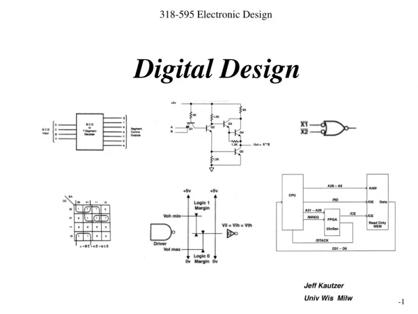
Advance Digital Design . Hassan Bhatti, Lecture 10. Field-Programmable Gate Arrays (FPGAs). Ease of reprogramming enable rapid prototyping Replacement of ASICs in low-volume end of the market Register rich tiled architecture of Functional units and a flexible channel based interconnections.

Advance Digital Design
E N D
Presentation Transcript
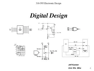
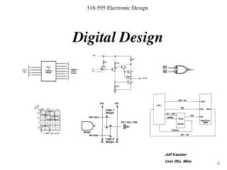
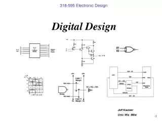
Advance Digital Design Hassan Bhatti, Lecture 10
Field-Programmable Gate Arrays (FPGAs) • Ease of reprogramming enable rapid prototyping • Replacement of ASICs in low-volume end of the market • Register rich tiled architecture of Functional units and a flexible channel based interconnections
Overview Continued • ASIC Research center has xess boards with Xilinx chips on them. • Every Xilinx chip required Xilinx tool to be compiled
FPGA Big Idea • Basic idea: 2D array of combination logic blocks (CL) and flip-flops (FF) with a means for the user to configure both: • the interconnection between the logic blocks, • the function of each block.
Idealized FPGA Logic Block • 4-input Look Up Table (4-LUT) • implements combinational logic functions • Register • optionally stores output of LUT • Latch determines whether read reg or LUT
Xilinx FPGA • Xilinx are pioneers in FPGA, launch first XC4000 FPGA in 1985. • Other generations like Spartan/XL etc are based on XC 4000. • Each FPGA consist of • Configurable Logic Blocks CLBs, • Routing Resources, • IOB (Input Output Buffers) • SRAM Based controller.
Architecture of CLBs • Each CLB has two 4-input Lookup Tables (LUTs) and two registers. • The two LUTs implement two independent logic functions F and G. • The outputs F’ and G’ from the two LUTs inside each CLB can be combined to form a more complex function H. • CLBs are linked together to form carry and cascade chain circuits not shown in diagram).
Interconnect Resources of XC 4000 • There are three types of interconnects • Dedicated Inter connects (Direct) : Lines provide routing b/w adjacent vertical and horizontal CLBs in the same row and column. • Double Length Lines: (Long lines) Transverse the distance of two CLBs before entering a switch matrix skipping every other CLBs. • Long Lines Span (Global): The entire array vertically and horizontally. They have splitters that segment the lines.
Architecture Of PIP • Break Point PIP • Connect or isolates two wire segments • Cross point PIP • Turn Corners • Multiplex PIP • Directional and buffered • Select one of n input to output
Example • Implement the following functions on a single • CLB of the XC4000 FPGA: • X = A’B’ (C + D) • Y = AK + BK + C’D’K + AEJL • Use look up table F to implement X • Use look up table G for AEJL • Use F, G and H for Y: • Y = K(A+B + C’D’) + AEJL • = KX’ + AEJL= KF’+G
Spartan 2 • ASIC Center got Xess-100 which has spartan-2 board. • The architecture is based on XC-4000.
Spartan-3E ArchitectureFundamental Elements • Configurable Logic Blocks (CLBs) • Consists of RAM based look up table to implement logic and storage elements that can be used as flip-flops or latches. • Input Output Blocks (IOBs) • Controls the flow of data between IO pins and internal logic. Supports many different signal standards. (Tri-state, bidirectional, LVTTL, etc. • Block RAM (BRAM) • 18 bit Multiplier Blocks • Digital Clock Manager (DCM)
Spartan 3 Configurable Logic Blocks (CLB’s) • CLBs contain Ram based lookup tables to implement logic and storage elements that can be used as flip-flops or latches. • CLBs can be programmed to perform a wide variety of logic functions as well as store data.
Spartan 3E IO Blocks (IOB’s) • IOB’s control flow of data between IO pins and the internal logic. • Each IOB supports bidirectional data flow, 3-state operation, and numerous different signal standards. (We will typically use LVTTL). See data sheet.
• Very low cost, high-performance logic solution for high-volume, consumer-oriented applications • Multi-voltage, multi-standard SelectIO™ interface pins - Up to 376 I/O pins or 156 differential signal pairs - LVCMOS, LVTTL, HSTL, and SSTL single-ended signal standards - 3.3V, 2.5V, 1.8V, 1.5V, and 1.2V signaling
Virtex Basic Architecture I/O Blocks (IOBs) Block SelectRAM™ resource Programmable interconnect Dedicated multipliers Configurable Logic Blocks (CLBs) Clock Management (DCMs, BUFGMUXes)
BUFT BUF T Slices and CLBs • Each Virtex-II CLB contains four slices • Local routing provides feedback between slices in the same CLB, and it provides routing to neighboring CLBs • A switch matrix provides access to general routing resources Switch Matrix Slice S3 Slice S2 SHIFT Slice S1 Slice S0 Local Routing CIN CIN
Slice Structure • The next few slides discuss the slice features • LUTs • MUXF5, MUXF6, MUXF7, MUXF8 (only the F5 and F6 MUX are shown in this diagram) • Carry Logic • MULT_ANDs • Sequential Elements
Combinatorial Logic A B Z C D Look-Up Tables • Combinatorial logic is stored in Look-Up Tables (LUTs) • Also called Function Generators (FGs) • Capacity is limited by the number of inputs, not by the complexity • Delay through the LUT is constant
F8 F5 F6 F5 F7 F5 F6 F5 Connecting Look-Up Tables MUXF8 combines the two MUXF7 outputs (from the CLB above or below) CLB Slice S3 MUXF6 combines slices S2 and S3 Slice S2 MUXF7 combines the two MUXF6 outputs Slice S1 MUXF6 combines slices S0 and S1 Slice S0 MUXF5 combines LUTs in each slice
COUT COUT To S0 of the next CLB To CIN of S2 of the next CLB SLICE S3 First Carry Chain CIN COUT SLICE S2 SLICE S1 CIN Second Carry Chain COUT SLICE S0 CIN CIN CLB Fast Carry Logic • Simple, fast, and complete arithmetic Logic • Dedicated XOR gate for single-level sum completion • Uses dedicated routing resources • All synthesis tools can infer carry logic
MULT_AND Gate • Highly efficient multiply and add implementation • Earlier FPGA architectures require two LUTs per bit to perform the multiplication and addition • The MULT_AND gate enables an area reduction by performing the multiply and the add in one LUT per bit LUT A CY_MUX CO S DI CI CY_XOR MULT_AND A x B LUT B LUT
_1 FDRSE D S Q CE R FDCPE D PRE Q CE CLR LDCPE D PRE Q CE G CLR Flexible Sequential Elements • Either flip-flops or latches • Two in each slice; eight in each CLB • Inputs come from LUTs or from an independent CLB input • Separate set and reset controls • Can be synchronous or asynchronous • All controls are shared within a slice • Control signals can be inverted locally within a slice
D Q CE D Q CE D Q CE D Q LUT CE Shift Register LUT (SRL16CE) • Dynamically addressable serial shift registers • Maximum delay of 16 clock cycles per LUT (128 per CLB) • Cascadable to other LUTs or CLBs for longer shift registers • Dedicated connection from Q15 to D input of the next SRL16CE • Shift register length can be changed asynchronously by toggling address A LUT D CE CLK Q A[3:0] Q15 (cascade out)
IOB Element • Input path • Two DDR registers • Output path • Two DDR registers • Two 3-state enable DDR registers • Separate clocks and clock enables for I and O • Set and reset signals are shared IOB Input Reg DDR MUX Reg OCK1 ICK1 Reg Reg 3-state OCK2 ICK2 Reg DDR MUX PAD OCK1 Reg Output OCK2
SelectIO Standard • Allows direct connections to external signals of varied voltages and thresholds • Optimizes the speed/noise tradeoff • Saves having to place interface components onto your board • Differential signaling standards • LVDS, BLVDS, ULVDS • LDT • LVPECL • Single-ended I/O standards • LVTTL, LVCMOS (3.3V, 2.5V, 1.8V, and 1.5V) • PCI-X at 133 MHz, PCI (3.3V at 33 MHz and 66 MHz) • GTL, GTLP • and more!
Digital ControlledImpedance (DCI) • DCI provides • Output drivers that match the impedance of the traces • On-chip termination for receivers and transmitters • DCI advantages • Improves signal integrity by eliminating stub reflections • Reduces board routing complexity and component count by eliminating external resistors • Eliminates the effects of temperature, voltage, and process variations by using an internal feedback circuit
Other Virtex-II Features • Distributed RAM and block RAM • Distributed RAM uses the CLB resources (1 LUT = 16 RAM bits) • Block RAM is a dedicated resources on the device (18-kb blocks) • Dedicated 18 x 18 multipliers next to block RAMs • Clock management resources • Sixteen dedicated global clock multiplexers • Digital Clock Managers (DCMs)
Distributed SelectRAM Resources • Uses a LUT in a slice as memory • Synchronous write • Asynchronous read • Accompanying flip-flops can be used to create synchronous read • RAM and ROM are initialized duringconfiguration • Data can be written to RAMafter configuration • Emulated dual-port RAM • One read/write port • One read-only port RAM16X1S D LUT WE WCLK A0 O A1 A2 A3 RAM32X1S RAM16X1D D D WE WE Slice WCLK WCLK A0 O A0 SPO LUT A1 A1 A2 A2 A3 A3 A4 DPRA0 DPO DPRA1 DPRA2 LUT DPRA3
Block SelectRAM Resources • Up to 3.5 Mb of RAM in 18-kb blocks • Synchronous read and write • True dual-port memory • Each port has synchronous read and write capability • Different clocks for each port • Supports initial values • Synchronous reset on output latches • Supports parity bits • One parity bit per eight data bits 18-kb block SelectRAM memory DIA DIPA ADDRA WEA ENA SSRA DOA CLKA DOPA DIB DIPB ADDRB WEB ENB SSRB DOB CLKB DOPB
Dedicated Multiplier Blocks • 18-bit twos complement signed operation • Optimized to implement Multiply and Accumulate functions • Multipliers are physically located next to block SelectRAM™ memory 18 x 18 Multiplier Data_A (18 bits) Output (36 bits) Data_B (18 bits)