Chapter 4: Processor Design
Chapter 4: Processor Design. Topics 4.1 The Design Process 4.2 A 1-Bus Microarchitecture for the SRC 4.3 Data Path Implementation 4.4 Logic Design for the 1-Bus SRC 4.5 The Control Unit 4.6 The 2- and 3-Bus Processor Designs 4.7 The Machine Reset 4.8 Machine Exceptions.

Chapter 4: Processor Design
E N D
Presentation Transcript
Chapter 4: Processor Design Topics 4.1 The Design Process 4.2 A 1-Bus Microarchitecture for the SRC 4.3 Data Path Implementation 4.4 Logic Design for the 1-Bus SRC 4.5 The Control Unit 4.6 The 2- and 3-Bus Processor Designs 4.7 The Machine Reset 4.8 Machine Exceptions
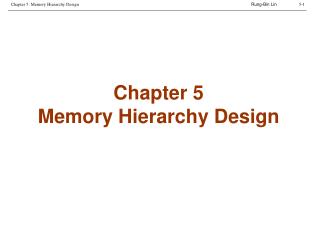
High-Level View of the 1-BusSRC Design ADD SUB AND OR SHR SHRA SHL SHC NOT NEG C=B INC4 12
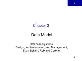
3 1 . . 0 3 1 0 R 0 3 1 0 3 2 3 2 - b i t 3 2 g e n e r a l P C p u r p o s e r e g i s t e r s R 3 1 I R A M A A B T o m e m o r y s u b s y s t e m A L U M D C C Constraints Imposed by the Microarchitecture • One bus connecting most registers allows many different RTs, but only one at a time • Memory address must be copied into MA by CPU • Memory data written from or read into MD • First ALU operand always in A, result goes to C • Second ALU operand always comes from bus • Information only goes into IR and MA from bus • A decoder (not shown) interprets contents of IR • MA supplies address to memory, not to CPU bus
3 1 . . 0 3 1 0 R 0 3 1 0 3 2 3 2 - b i t 3 2 g e n e r a l P C p u r p o s e r e g i s t e r s R 3 1 I R A M A A B T o m e m o r y s u b s y s t e m A L U M D C C Abstract and Concrete RTN for SRCadd Instruction Abstract RTN: (IR M[PC]: PC PC + 4; instruction_execution); instruction_execution := ( • • • add (:= op= 12) R[ra] R[rb] + R[rc]: • Parts of 2 RTs (IR M[PC]: PC PC + 4;) done in T0 • Single add RT takes 3 concrete RTs (T3, T4, T5) Concrete RTN for the add instruction Step RTN T0 MAPC: C PC + 4; T1 MD M[MA]: PC C; T2 IR MD; T3 A R[rb]; T4 C A + R[rc]; T5 R[ra] C; IF IEx.
Concrete RTN Gives Information About Sub-units • The ALU must be able to add two 32-bit values • ALU must also be able to increment B input by 4 • Memory read must use address from MA and return data to MD • Two RTs separated by : in the concrete RTN, as in T0 and T1, are operations at the same clock • Steps T0, T1, and T2 constitute instruction fetch, and will be the same for all instructions • With this implementation, fetch and execute of the add instruction takes 6 clock cycles
3 1 . . 0 3 1 0 R 0 3 1 0 3 2 3 2 - b i t 3 2 g e n e r a l P C p u r p o s e r e g i s t e r s R 3 1 I R A M A A B T o m e m o r y s u b s y s t e m A L U M D C C Concrete RTN for Arithmetic Instructions: addi Abstract RTN: addi (:= op= 13) R[ra] R[rb] + c216..0{2's complement sign extend} : • Differs from add only in step T4 • Establishes requirement for sign extend hardware Concrete RTN for addi: Step RTN T0. MAPC: C PC + 4; T1. MD M[MA]; PC C; T2. IR MD; T3. A R[rb]; T4. C A + c216..0 {sign ext.}; T5. R[ra] C; Instr Fetch Instr Execn.
More Complete View of Registers and Buses in the 1-Bus SRC Design, Including Some Control Signals • Concrete RTN lets us add detail to the data path • Instruction register logic and new paths • Condition bit flip-flop • Shift count register
Abstract and Concrete RTN forLoad and Store • ld (:= op= 1) R[ra] M[disp] : • st (:= op= 3) M[disp] R[ra] : • where • disp31..0 := ((rb=0) c216..0 {sign ext.} : • (rb0) R[rb] + c216..0 {sign extend, • 2's comp.} ) : The ld and St Instructions Step RTN for ld RTN for st T0–T2 Instruction fetch T3 A (rb = 0 0: rb 0 R[rb]); T4 C A + (16@IR16#IR15..0); T5 MA C; T6 MD M[MA]; MD R[ra]; T7 R[ra] MD; M[MA] MD;
Concrete RTN for Conditional Branch br (:= op= 8) (cond PC R[rb]): cond := ( c32..0=0 0: never c32..0=1 1: always c32..0=2 R[rc]=0: if register is zero c32..0=3 R[rc]0: if register is nonzero c32..0=4 R[rc]31=0: if positive or zero c32..0=5 R[rc]31=1 ): if negative The Branch Instruction, br Step RTN T0–T2 Instruction fetch T3 CON cond(R[rc]); T4 CON PC R[rb];
Abstract and Concrete RTN for SRC Shift Right shr (:= op = 26) R[ra]31..0 (n @ 0) # R[rb]31..n : n := ( (c34..0= 0) R[rc]4..0 : Shift count in register (c34..0 0) c34..0 ): or constant field of instruction The shr Instruction Step Concrete RTN T0–T2 Instruction fetch T3 n IR4..0; T4 (n = 0) (n R[rc]4..0 T5C R[rb]; T6 Shr (:= (n 0) (C31..0 0#C31..1 n n - 1; Shr) ); T7 R[ra] C; step T6 is repeated n times
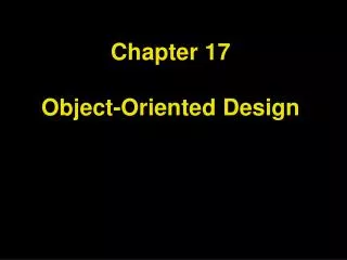
B u s . . . b < 3 1 . . . 0 > 3 1 2 6 2 7 2 2 2 1 1 7 1 6 1 2 1 1 . . . O p r a r b r c I R 2 3 2 5 5 5 1 G r a G r b G r c 3 2 Q D 3 3 2 6 R 3 1 5 5 5 5 Q 3 2 8 5 . . . F r o m F i g u r e 4 . 3 3 2 3 1 0 r 3 1 e R 0 1 R 3 1 d 3 2 3 2 3 2 - b i t o D Q 3 2 c g e n e r a l e 3 2 . . . 6 p u r p o s e R 1 d 5 5 r e g i s t e r s S e l e c t l o g i c 2 Q 1 3 I R o R 1 t R 3 1 5 3 2 8 0 4 R 0 1 3 2 3 2 D Q 3 2 R 0 6 5 R Q i n R o u t 7 B A o u t The Register File and Its Control Signals • Rout gates selectedregister onto bus • Rin strobed selectedregister from bus • BAout differs from Rout by gating 0 when R[0] is selected BA = Base Address
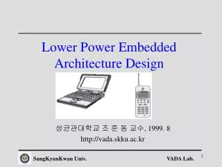
Extracting c1, c2, and OP from the Instruction Register, IR<31...0> • I21 is the sign bit of C1 that must be extended • I16 is the sign bit of C2 that must be extended • Sign bits are fanned out from one to several bits and gated to bus
3 2 3 2 M D 3 2 3 2 3 2 b u s D Q 1 M D r d M D R e a d 3 2 3 2 Q F r o m F i g u r e 4 . 3 W r i t e 2 3 M D 3 1 . . 0 S t r o b e D o n e M A 3 2 T o m e m o r y s u b s y s t e m 3 2 d a t a 3 1 . . 0 M D M D w r M e m o r y M D o u t b u s a d d r 3 1 . . 0 3 2 3 2 D Q M A M A Q i n C P U b u s M A 3 1 . . 0 The CPU–Memory Interface: Memory Address and Memory Data Registers, MA<31...0> and MD<31...0> • MD is loaded from memory or fromCPU bus • MD can drive CPU bus or memory bus
3 2 D Q A 3 2 A F r o m F i g u r e 4 . 3 Q i n A A D D A B A L U A B S U B C A N D . . . 1 1 3 2 A L U C N O T C = B C I N C 4 3 2 3 2 D Q C C o u t C Q i n The ALU and Its Associated Registers
From Concrete RTN to Control Signals: The Control Sequence The Instruction Fetch • The register transfers are the concrete RTN • The control signals that cause the register transfers make up the control sequence • Wait prevents the control from advancing to step T3 until the memory asserts Done Step Concrete RTN Control Sequence T0 MA PC: C PC + 4; PCout, MAin, INC4, Cin T1 MD M[MA]: PC C; Read, Cout, PCin, Wait T2 IR MD; MDout, IRin T3 Instruction_execution
Control Steps, Control Signals, and Timing • Within a given time step, the order in which control signals are written is irrelevant • In step T0, Cin, Inc4, MAin, PCout == PCout, MAin, INC4, Cin • The only timing distinction within a step is between gates and strobes • The memory read should be started as early as possible to reduce the wait • MA must have the right value before being used for the read • Depending on memory timing, Read could be in T0
Control Sequence for the SRC add Instruction add (:= op = 12) R[ra] R[rb] + R[rc]: The add Instruction • Note the use of Gra, Grb, and Grc to gate the correct 5-bit register select code to the registers • End signals the control to start over at step T0 Step Concrete RTN Control Sequence T0 MA PC: C PC + 4; PCout, MAin, INC4, Cin, Read T1 MD M[MA]: PC C; Cout, PCin, Wait T2 IR MD; MDout, IRin T3 A R[rb]; Grb, Rout, Ain T4 C A + R[rc]; Grc, Rout, ADD, Cin T5 R[ra] C; Cout, Gra, Rin, End
Control Sequence for the SRC addi Instruction addi (:= op= 13) R[ra] R[rb] + c216..0 {2’s comp., sign ext.} : • The c2out signal sign extends IR16..0 and gates it to the bus The addi Instruction Step Concrete RTN Control Sequence T0. MA PC: C PC + 4; PCout, MAin, Inc4, Cin, Read T1. MD M[MA]; PC C; Cout, PCin, Wait T2. IR MD; MDout, IRin T3. A R[rb]; Grb, Rout, Ain T4. C A + c216..0 {sign ext.}; c2out, ADD, Cin T5. R[ra] C; Cout, Gra, Rin, End
Control Sequence for the SRC st Instruction • st (:= op = 3) M[disp] R[ra] : • disp31..0 := ((rb=0) c216..0 {sign extend} : • (rb0) R[rb] + c216..0 {sign extend, 2’s complement} ) : • Note BAout in T3 compared to Rout in T3 of addi The st Instruction Step Concrete RTN Control Sequence T0–T2 Instruction fetch Instruction fetch T3 A (rb=0) 0: rb 0 R[rb]; Grb, BAout, Ain T4 C A + c216..0 {sign-extend}; c2out, ADD, Cin T5 MA C; Cout, MAin T6 MD R[ra]; Gra, Rout, MDin, Write T7 M[MA] MD; Wait, End
B u s . . . b < 3 1 . . . 0 > 3 1 2 6 2 7 2 2 2 1 1 7 1 6 1 2 1 1 . . . O p r a r b r c I R 2 3 2 5 5 5 1 G r a G r b G r c 3 2 Q D 3 3 2 6 R 3 1 5 5 5 5 Q 3 2 8 5 . . . F r o m F i g u r e 4 . 3 3 2 3 1 0 r 3 1 e R 0 1 R 3 1 d 3 2 3 2 3 2 - b i t o D Q 3 2 c g e n e r a l e 3 2 . . . 6 p u r p o s e R 1 d 5 5 r e g i s t e r s S e l e c t l o g i c 2 Q 1 3 I R o R 1 t R 3 1 5 3 2 8 0 4 R 0 1 3 2 3 2 D Q 3 2 R 0 6 5 R Q i n R o u t 7 B A o u t The Register File and Its Control Signals • Rout gates selectedregister onto bus • Rin strobed selectedregister from bus • BAout differs from Rout by gating 0 when R[0] is selected BA = Base Address
The Shift Counter • The concrete RTN for shr relies upon a 5-bit register to hold the shift count • It must load, decrement, and have an = 0 test B u s F r o m F i g u r e 4 . 3 5 4 . . 0 4 0 4 . . 0 n : s h i f t c o u n t n = 0 n 3 2 D e c r 5 - b i t d o w n c o u n t e r D e c r e m e n t S h i f t c o u n t , n n = Q 4 . . Q 0 L d 3 1 . . 0 n = 0
Control Sequence for the SRC shr Instruction—Looping • Conditional control signals and repeating a control step are new concepts • Step Concrete RTN Control Sequence • T0–T2 Instruction fetch Instruction fetch • T3 n IR4..0; c1out, Ld • T4 (n=0) (n R[rc]4..0); n=0 (Grc, Rout, Ld) • T5 C R[rb]; Grb, Rout, C=B, Cin • T6 Shr (:= (n0) n0 (Cout, SHR, Cin, • (C31..0 0#C31..1: Decr, Goto6) • n n-1; Shr) ); • T7 R[ra] C; Cout, Gra, Rin, End
The ALU and Its Associated Registers 3 2 D Q A 3 2 A F r o m F i g u r e 4 . 3 Q i n A A D D A B A L U A B S U B C A N D . . . 1 2 3 2 A L U C N O T C = B C I N C 4 SHR 3 2 3 2 D Q C C o u t C Q i n
Branching cond := ( c32..0=0 0: c32..0= 1 1: c32..0= 2 R[rc] = 0: c32..0= 3 R[rc] 0: c32..0= 4 R[rc]31= 0: c32..0= 5 R[rc]31= 1 ): • This is equivalent to the logic expression cond = (c32..0= 1) (c32..0= 2)(R[rc] = 0) (c32..0= 3)(R[rc] = 0) (c32..0= 4)R[rc]31 (c32..0= 5)R[rc]31
Computation of the Conditional Value CON I R 2 . . 0 • NOR gate does = 0 test of R[rc] on bus 3 B u s D e c o d e r F r o m F i g u r e 4 . 3 5 4 3 2 1 0 0 D Q C O N 1 C O N i n 3 2 = 0 3 2 C o n d l o g i c 0 D Q c 3 2 . . 0 0 C O N 3 1 Q C O N i n < 0 3 1 . . 0
Control Sequence for SRC Branch Instruction, br br (:= op = 8) (cond PC R[rb]): • Condition logic is always connected to CON, so R[rc] only needs to be put on bus in T3 • Only PCin is conditional in T4 since gating R[rb] to bus makes no difference if it is not used Step Concrete RTN Control Sequence T0–T2 Instruction fetch Instruction fetch T3 CON cond(R[rc]); Grc, Rout, CONin T4 CON PC R[rb]; Grb, Rout, CON PCin, End
Summary of the Design Process Starting with informal description • formal RTN description • block diagram architecture • concrete RTN steps • hardware design of blocks • control sequences • control unit and timing • At each level, more decisions must be made • These decisions refine the design • Also place requirements on hardware still to be designed • The nice one-way process above has circularity • Decisions at later stages cause changes in earlier ones • Happens less in a text than in reality because • Can be fixed on re-reading • Confusing to first-time student
Clocking the Data Path: Register Transfer Timing L o g i c S o u r c e D e s t i n a t i o n B u s b l o c k r e g i s t e r g a t e r e g i s t e r n - b i t b u s D Q D Q • tR2valid is the period from begin of gate signal till inputs to R2 are valid • tcomb is delay through combinational logic, such as ALU or cond logic C o m b i n a t i o n a l n R 1 R 2 R l o g i c o u t C K C K Q Q R i n G a t e B u s p r o p . A L U , L a t c h C i r c u i t p r o p . d e l a y , e t c . p r o p . p r o p a g a t i o n t i m e , t d e l a y , d e l a y , d e l a y b p t t t g c o m b l G a t e s i g n a l : L a t c h h o l d t i m e , t h R o u t L a t c h s e t u p t i m e , t s u S t r o b e s i g n a l : t R 2 v a l i d R i n M i n i m u m p u l s e w i d t h , t w M i n i m u m c l o c k p e r i o d , t m i n
The Control Unit • The control unit’s job is to generate the control signals in the proper sequence • Things the control signals depend on • The time step Ti • The instruction opcode (for steps other than T0, T1, T2) • Some few data path signals like CON, n = 0, etc. • Some external signals: reset, interrupt, etc. (to be covered) • The components of the control unit are: a time state generator, instruction decoder, and combinational logic to generate control signals
Step C o n t r o l S e q u e n c e T0. P C , M A , I n c 4 , C , R e a d o u t i n i n T1. C , P C , W a i t o u t i n T2. M D , I R o u t i n a d d a d d i s t s h r C o n t r o l S e q u e n c e Step C o n t r o l S e q u e n c e Step C o n t r o l S e q u e n c e Step C o n t r o l S e q u e n c e T3. T3. T3. G r b , R , A G r b , R , A G r b , B A , A c 1 , L d o u t i n o u t i n o u t i n o u t T4. T4. T4. G r c , R , A D D , C c 2 , A D D , C c 2 , A D D , C n = 0 ( G r c , R , L d ) o u t i n o u t i n o u t i n o u t G r a , G r a , T5. T5. T5. C , M A G r b , R , C = B C , R , E n d C , R , E n d o u t i n o u t o u t i n o u t i n G r a , T6. T6. n 0 ( C , S H R , C , R , M D , W r i t e o u t i n o u t i n D e c r , G o t o 7 ) T7. W a i t , E n d G r a , T7. C , R , E n d o u t i n Synthesizing Control Signal Encoder Logic Design process: • Comb through the entire set of control sequences. • Find all occurrences of each control signal. • Write an equation describing that signal. Example: Gra = T5·(add + addi) + T6·st + T7·shr + ... Step T3. T4. T5.
Step C o n t r o l S e q u e n c e T0. P C , M A , I n c 4 , C , R e a d o u t i n i n T1. C , P C , W a i t o u t i n T2. M D , I R o u t i n a d d a d d i s t s h r Step C o n t r o l S e q u e n c e Step C o n t r o l S e q u e n c e Step C o n t r o l S e q u e n c e Step C o n t r o l S e q u e n c e T3. T3. T3. T3. G r b , R , A G r b , R , A G r b , B A , A c 1 , L d o u t i n o u t i n o u t i n o u t G r c , T4. T4. T4. n = 0 ( G r c , c 2 , A D D , C c 2 , A D D , C T4. R , A D D , C o u t i n o u t i n o u t i n R , L d ) o u t T5. T5. T5. C , G r a , R , E n d C , M A T5. C , G r a , R , E n d o u t i n o u t i n G r b , R , C = B o u t i n o u t T6. T6. G r a , R , M D , W r i t e o u t i n n 0 ( C , S H R , C , o u t i n T7. D e c r , G o t o 7 ) W a i t , E n d T7. C , G r a , R , E n d o u t i n Use of Data Path Conditions in Control Signal Logic Example: Grc = T4·add + T4·(n=0)·shr + ...
. . . . . . T 5 a d d T 1 a d d i G r a C o u t T 7 T 5 . . . . . . a d d l d Generation of the logic forCout and Gra
. Branching in the Control Unit • 3-state gates allow 6 to be applied to counter input • Reset will synchronously reset counter to step T0
The Clocking Logic:Start, Stop, and Memory Synchronization • Mck is master clock oscillator
The Complete 1-Bus Design of SRC • High-level architecture block diagram • Concrete RTN steps • Hardware design of registers and data path logic • Revision of concrete RTN steps where needed • Control sequences • Register clocking decisions • Logic equations for control signals • Time step generator design • Clock run, stop, and synchronization logic
Other Architectural Designs Will Requirea Different RTN • More data paths allow more things to be done in one step • Consider a two bus design • By separating input and output of ALU on different buses, the C register is eliminated • Steps can be saved by strobing ALU results directly into their destinations
A b u s B b u s 3 1 0 ( “ I n b u s ” ) ( “ O u t b u s ” ) R 0 3 2 3 2 3 2 g e n e r a l p u r p o s e r e g i s t e r s R 3 1 I R P C M A M e m o r y b u s M D A A B A L U C The 2-Bus SRC Microarchitecture • Bus A carries data going into registers • Bus B carries data being gated out of registers • ALU function C = B is used for all simple register transfers
A b u s B b u s 3 1 0 ( “ I n b u s ” ) ( “ O u t b u s ” ) R 0 3 2 3 2 3 2 g e n e r a l p u r p o s e r e g i s t e r s R 3 1 I R P C M A M e m o r y b u s M D A A B A L U C The 2-Bus add Instruction Step Concrete RTN Control Sequence T0 MA PC; PCout, C = B, MAin, Read T1 PC PC + 4: MD M[MA];PCout, INC4, PCin, Wait T2 IR MD; MDout, C = B, IRin T3 A R[rb]; Grb, Rout, C = B, Ain T4 R[ra] A + R[rc]; Grc, Rout, ADD, Sra, Rin, End • Note the appearance of Grc to gate the output of the register rc onto the B bus and Sra to select ra to receive data strobed from the A bus • Two register select decoders will be needed