Download
1 / 9
90 likes | 355 Views
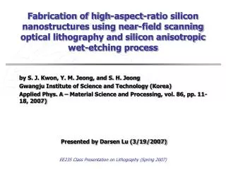
Fabrication of high-aspect-ratio silicon nanostructures using near-field scanning optical lithography and silicon anisotropic wet-etching process. by S. J. Kwon, Y. M. Jeong, and S. H. Jeong Gwangju Institute of Science and Technology (Korea)

E N D
Fabrication of high-aspect-ratio siliconnanostructures using near-field scanningoptical lithography and silicon anisotropicwet-etching process by S. J. Kwon, Y. M. Jeong, and S. H. Jeong Gwangju Institute of Science and Technology (Korea) Applied Phys. A – Material Science and Processing, vol. 86, pp. 11-18, 2007) Presented by Darsen Lu (3/19/2007) EE235 Class Presentation on Lithography (Spring 2007)
Outline • Introduction • Description of the tools and experimental setup • Fabrication Results • Conclusion EE235 Class Presentation on Lithography (Spring 2007)
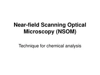
Introduction • Scanning probe lithography (SPL) • SPL is a nanopatterning technique based on scanning probe microscope technologies • Various forms of SPL techniques include • Atomic Force Microscope (AFM) Lithography • Dip-pen lithography • Near Field Scanning Optical lithography(NSOL) • As opposed to the electron beam (e-beam) lithography, SPLs can be exercised under ambient conditions • This Paper • The NSOL is used to pattern nanochannels with high aspect ratio EE235 Class Presentation on Lithography (Spring 2007)
Introduction Dip Pen Nanolithography Atomic Force Microscope http://www.nanoink.net/WhatisDPN.htm http://stm2.nrl.navy.mil/how-afm/how-afm.html Near Field Scanning Optical Microscopy In near field scanning optical microscopy (NSOM) a very small light source very close to the sample is scanned. Light passes through a sub-wavelength diameter aperture and illuminates a sample that is placed within its near field, at a distance much less than the wavelength of the light. The resolution achieved is far better than that which is attainable in conventional optical microscopes. http://en.wikipedia.org/wiki/Near-field_scanning_optical_microscope EE235 Class Presentation on Lithography (Spring 2007)
The Near-field scanning optical lithography (NSOL) system 442nm, 130mW, He-Cd Laser Source ND Filter Shutter • Light goes through the apertured cantilever nanoprobe and expose the photoresist (PR). • The nanoprobe moves along a trajectory to pattern the PR Fiber Position Feedback System Power Meter Motorized Stage Apertured Cantilever Nanoprobe Wafer + PR EE235 Class Presentation on Lithography (Spring 2007)
Fabrication process • Goal: fabricate high-aspect-ratio (HAR) nanochannels • Procedure: • Start with a 110 wafer • Deposit 10nm nitride using LPCVD • A commercial photoresist is deposited on the wafer • The 111 direction of the wafer is aligned precisely to the y-axis of the microscope • The NSOL scans through the programmed trajectory • PR Development • RIE etch of PR and nitride in CF4/O2 Plasma • KOH wet etch EE235 Class Presentation on Lithography (Spring 2007)
Results: After PR Development • Good linewidth uniformity is achieved (Fig. 1, 2) • Reproducibility over the same sample has been proved (Fig. 3) • Reproducibility between different samples requires further study (Fig. 4) • Solid lines: first sample • Dotted lines: second sample 13% Fig. 3 7.7% Fig. 1 Fig. 2 Fig. 4 EE235 Class Presentation on Lithography (Spring 2007)
Result: After KOH wet etching • Wet Etching Result 1. Width 200nm / Depth 800nm 2. Width 230nm / Depth 1560nm • Compare with theoretical KOH selectivity • Reason for width increase: • Nonzero etching in the {111} plane • Thinning of Si3N4 at the edge of the channel during the dry-etching • The. {111} : {110} = 1 : 600 • Exp. {111} : {110} = 1 : 26 • NSOL effect was proven by closing the shutter during the scanning process (see right figure) EE235 Class Presentation on Lithography (Spring 2007)
Summary • An NSOL system has been set up for nanofabrication • Lines have been patterned and good linewidth uniformity has been demonstrated. However, further study is needed to improve the reproducibility over different samples. • Nanochannel has been produced after wet etching. A linewidth of ~200nm and an aspect ratio of 1:6.8 has been achieved. • This nanofabrication technology could be potentially applicable to the fabrication of micro/nanofluidic channels, substrates for biomolecular analysis, etc. EE235 Class Presentation on Lithography (Spring 2007)