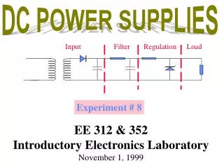

Experiment 8
E N D
Presentation Transcript
Experiment 8 Counting with Sequential Logic
Experiment 7 Questions 1. Determine the propagation delay (in number of gates) from each input to each output for the half adder. One gate delay maximum. 2. Determine the propagation delay (in number of gates) from each input to each output for the full adder. Two gates delays. 3. How many rows would there be in the truth table for a 4-bit binary adder? 32 rows How many input and output variables are there? 8 input; 5 output Would it be feasible to design a 32-bit adder using this technique? Not in this lifetime 4. How many logic gates are needed to build the 4-bit ripple carry adder? 2 + 3*6 = 20 What is the worst case delay path through the 4-bit ripple carry adder? When a carry propagates through each of the bits. What 4-bit input values cause the worst case delay? 1111 + 0001 (and others) 5. List the number of gate delays that are on the critical path? 4-bit RCA = 7 gates delays How many gate delays would there be in an 8-bit ripple carry adder? 15 gate delays. 6. How many gate delays would there be in an n-bit ripple carry adder? 2(n-1) + 1 How would you modify your 4-bit ripple carry adder to make an adder/subtractor? Change half adder to full adder, be able to complement one operand (2’s complement approach).
Experiment 7 Comments • Directly reference figures and tables • Indirectly reference VHDL code and timing diagrams • Efficiency of Ripple carry adder • time efficient? NO • space efficient? YES
Instructional Objectives: • To use sequential VHDL statements in the design of flip-flops • To design a T flip-flop • To design a T-FF based 4-bit counter • To use the LA to verify 4-bit counter
Sequential Storage Elements • Combinatorial vs. Sequential Circuits • Combinatorial: cannot store information • Outputs a function of inputs • Sequential: stores information (bits) • Outputs a function of inputs and current outputs • Sequential Circuits: considered to have states • State of circuit: based on what is being store by circuits storage elements • Sequential circuits = finite state machines (FSMs)
Basic Bit-Storage Elements • Latches • Cross coupled cells: NOR and NAND • state changes when inputs change • Gated latches (add a clock) • State changes on active level of clock • Level sensitive devices • Flip-flops • State changes only on active edge of clock signal • RET (rising-edge triggered devices) • FET (falling-edge triggered devices)
D Flip-flop A D flip-flop changes its current state Q at the rising edge of a clock signal. It’s new state is given by the characteristic equation of the D flip-flop: Q+ = D (Q+ = next state of circuit)
T T Flip-flop A T flip-flop changes its current state Q at the rising edge of a clock signal. It’s new state is given by the characteristic equation of the T flip-flop: Q+ = T XOR Q (Q+ = next state of circuit)
VHDL Sequential Statements ARCHITECTURE my_arch OF myhalfadder IS BEGIN PROCESS (sensitivity list) BEGIN sequential statement 1; sequential statement 2; END PROCESS; END my_arch;
Experiment 8 Overview P1: Implement a T flip-flop P2: Implement a 4-bit counter using your T flip-flop module and any additional gates. P3: Analyze your circuit with the Logic Analyzer