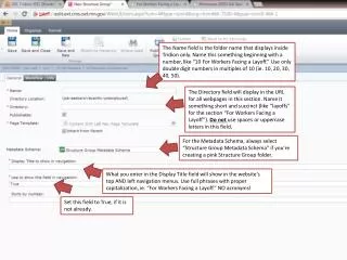
Download
1 / 42
490 likes | 951 Views
場發射顯示器之展望 The Prospects of Field Emission Displays 大同公司 FED 研發處 羅吉宗 處長. 簡 報 內 容. ◆ FED vs other displays. ◆ What is the Field Emission Display (FED)﹖ ◆ Kinds of field emission display. The traditional FEDs — PixTech, Motorola, Candescent/Sony, Futaba.

E N D
場發射顯示器之展望The Prospects of Field Emission Displays大同公司 FED研發處 羅吉宗 處長
簡 報 內 容 • ◆ FED vs other displays. • ◆ What is the Field Emission Display (FED)﹖ • ◆ Kinds of field emission display. • The traditional FEDs — PixTech, Motorola, Candescent/Sony, Futaba. • The New Approaches — pFED, SED and CNT FED. ◆The prospects of commercial FED.
簡 報 內 容 • ◆ FED vs other displays. • ◆ What is the Field Emission Display (FED)﹖ • ◆ Kinds of field emission display. ●The traditional FEDs — PixTech, Motorola, Candescent/Sony, Futaba. ●The New Approaches —pFED, SED and CNT FED ◆ The prospects of commercial FED.
FED與其他類型顯示器之特性比較 ●: good ; ○:medium ; X : bad
FED產品定位 Different Technologies & their limitations TFT-LCD Existing Technologies Complex vacuum process, yield problems as size increases CRT PDP Various Pixel Module Display Bulky, large screens costly to manufacture Power hungry, inefficient as smaller screen, expensive electronics Relative expensive to mfg.& operate, separate pixels-discontinuous & heavy panel 1” 10” 20” 30” 40” 50” 60” Screen Diagonal Source: Materials World, Vol. 8, pp22-25 OLED Tip FED Flat FED Printable FED Emerging Technologies
數位電視將為未來家庭娛樂、資訊及控制中心 場發射顯示技術將發展出HDTV、大型戶外看板、面光源、投影光源、X-ray醫療裝置、STM等產品。
簡 報 內 容 • ◆ FED vs other displays. • ◆ What is the Field Emission Display (FED)﹖ • ◆ Kinds of field emission display. ●The traditional FEDs — PixTech, Motorola, Candescent/Sony, Futaba. ●The New Approaches —pFED, SED and CNT FED ◆ The prospects of commercial FED.
CRT >400mm • Cross-Section of an FED • 1. Dielectric • 2. Patterned Resister Layer • 3. Cathode Glass • 4. Row Metal • 5. Emitter Array • 6. Single Emitter Cone & Gate Hole • 7. Column Metal • 8. Focusing Grid • 9. Wall • 10. Phosphor • 11. Black Matrix • 12. Aluminum Layer • 13. Pixel On • 14. Faceplate Glass FED 10~30mm CRT → Field Emission Display 1.CRT與FED都是以電子激發螢光粉而發光(CL)之裝置。 2.CRT是電子槍之熱電子發射,而FED是藉電場作用之冷電子穿隧。
◆CRT是熱電子發射。Richardson熱燈絲電流密度 Richardson const. , 為導體表面之功函 數,在外加電場Eext作用下,表面能障降低 。 ◆FED是冷電子穿隧,高電場作用下,導體表面有效能障 降低,障壁變薄,電子易穿隧。Fowler-Nordheim穿隧電流 密度 ,A、B為常數,電場 ,ß 是電場放大因子,它與emitter形狀有關。
FED基本結構與操作原理 CNT
FED基本結構與操作原理 • FED陽極顯示面板上,紅、綠、藍三個色素被black matrix隔開,每一畫素(pixel)都與陰極之一場發射電子源對應,陰極上的電子源受閘極控制開或關。 • FED在畫素需要顯示時,加上該畫素電壓的瞬間即可發射穿隧電子,穿隧電子的電流密度很低,驅動電路不必很複雜,因此功率消耗很低。 • FED在真空中Gate極加電場使emitter表面發射電子,陽極電壓加速電子激發螢光粉材料而發光,具有與CRT相同之CL優美畫質,因此可說FED是平面化之CRT。 • FED是百萬畫素之多電子源直接激發銀幕上之螢光材料,不必像CRT需藉磁場控制自電子槍射出之電子束路徑,因此CRT之陰極到陽極距離需400mm而FED只需1mm左右。
FED基本結構與操作原理 • CRT的電子槍提供25KeV之電子束激發陽極之螢光材料僅是能量轉移,而FED的陽極加速電壓除提供電子能量激發螢光材料,螢光材料也受到電子撞擊力,因此FED需開發高效率之低電壓螢光粉。 • 因此FED是很薄、低功率消耗、視角廣、適用溫度很寬、可 • 快速播放、有HDTV畫質之平板顯示器。 • 場發射顯示器之技術要求: • FED的電功率消耗低,要面板之操作電壓低,電子發射材料之起始電場越低越好。 • 滿足解析度需求,電子發射位置密度(ESD)需大於106cm-2。每個畫素之電子源分布需均勻發射電子。 • 在高真空、高電壓下維持輝光穩定性與元件壽命之技術與成本,決定產品之競爭力。
簡 報 內 容 • ◆ FED vs other displays. • ◆ What is the Field Emission Display (FED)﹖ • ◆ Kinds of field emission display. ●The traditional FEDs — PixTech, Motorola, Candescent/Sony, Futaba. ●The New Approaches —pFED, SED and CNT FED ◆ The prospects of commercial FED.
Spindt Type FED Typical System Design of Spindt-FED
Spindt Type FED PixTech FED PixTech 5.2” In field emission displays, electrons coming from millions of tiny micro-tips pass through gates and light up pixels on a screen.
Spindt Type FED 美國Micron Display Technology (MDT)是以直徑25µm,長度350µm之玻璃纖維直接結合在陽極板或陰極板之間,其配列之間距為100µm (如圖一)。此種圓柱設計的優點是提供足夠的抽氣通路,使得後續真空封合可以順利進行。 其最大的缺點則在於單支玻璃纖維之垂直度並不易維持,這是因為在真空封合製程中,由於壓力差極易產生橫向剪力,而圓柱結構形式是最無法承受剪力,易於造成垂直度不良。垂直度良好方能確保在另一面板(陽極板或陰極板)上,也獲得正確的定位,而不會造成混色問題。 另外在高溫結合製程中,易於因製程溫度差異而造成最後成品收縮,導致位置精度不足,也會造成混色問題。另一缺點是,其製作仍需搭配前後製程,無法分離,在成本上不易降低,對於未來普及化的幫助有限。 PixTech FED 美國 Micron Display Technology 發展之FED Spacer Posts
Spindt Type FED Motorola
Spindt Type FED Spacer Wall 美國 Candescent 與日本 Sony 共同發展之 FED 美國Candescent與日本Sony於2000年5月之SID年會中共同發展之FED尺寸,已由5.3”提昇至13.2”。其Spacer是採用長壁(Wall)方式,為壁厚55µm,壁高1270µm,壁長278mm之陶瓷板,其Spacer高寬比為23。擺置方式採用水平橫式放置在畫素與畫素之間隙上。
Spindt Type FED Candescent ThinCRT Technology Image from 13.2 in. SVGA 18-bit color Sony/Candescent Joint Development Display
Spindt Type FED Futaba (14.4”SVGA / 2005)
Why the traditional FEDs are going out? Cost, Cost, Cost, ... ◆ Small Size Display Only High Voltage Driver IC Spacer Technology Low Throughput Self-AlignedSpindt Emitter IC Process
What’s next? ◆ Large Size Display Possible Lower Voltage Driver IC Improved Spacer Technology Thin Film Technology Printing Process
簡 報 內 容 • ◆ FED vs other displays. • ◆ What is the Field Emission Display (FED)﹖ • ◆ Kinds of field emission display. ●The traditional FEDs — PixTech, Motorola, Candescent/Sony, Futaba. ●The New Approaches —pFED, SED and CNT FED ◆ The prospects of commercial FED.
PFE-pFED Phosphor coated anode Printed gate electrode Printed gate insulator Printed PFE emitter layer Variable negative voltage applied to modulate current to produce picture Printed emitter track Etch stop Active emitter exposed at bottom of cells Positive voltage applied to select line Single exposure self-aligning Glass substrate etch system for emitter-cells ~ 10 micron in diameter pFED
pFED PFE-pFED PFE的FED陰極板結構是將導體或半導體(可能是graphite、DLC或CNT)配成漿料後,以網印技術印在玻璃基板之電極上,燒結後發射源厚度約1um,而導電粒子上覆蓋約10nm厚之絕緣層。 接著在emitter上,塗布gate oxide和gate電極,然後以光罩和微影蝕刻技術,gate電極和gate oxide被挖出小孔,閘極上加電壓則emitter之電子將穿隧透過小孔,被陽極電場加速撞擊螢光材料而發光。 Emitter網印層中陰極電子以MIM進入導電粒子,再以MIV穿隧入真空然後跑到陽極,此結構可維持emitter壽命很長。
pFED PFE-pFED Conducting or semi-conducting particle. Typically graphite Electron emission MIV channel Insulating matrix often silica MIM channel Optional resistive layer Substrate Conducting layer The Electron Emission Mechanism PFE emitter technology utilises the source of pre-breakdown current PFE’s Screen Printable Cold Cathode – MIMIV Structure
Hop-FED • Derived from Philips’ Zeus Project • Homogenises and focuses electrons • Many benefits in panel performance and handling Hop-Plate New pFED™ design with Hop-Plate PFE導入Philip之技術,在陰極板之電子發射孔上加一層Hop-Plate。Hop-Plate除了當spacer外,也可改善色純度和畫素內電子分布均勻性,。
Hop-Flue FED PFE-pFED Anode Plane Conducting Layer Phosphor dots (~ +5kV to+10kV) Hop Electrode (~ +325V) Flue-channel With anti-flashover coating Hop-channel Gate Electrode (~ +175V) Flue Spacer Hop Spacer The Hop-FED homogenises and focuses the output of many emitting sites 同樣以噴砂技術,在Hop-Plate上再放一噴出小孔的Flue-Plate,孔內鍍防arcing薄膜,它引導自Hop-Plate出來的電子直接打在螢光材料上,即Flue-Plate當spacer又可使電子聚焦改善色純度。
Hop-FED PFE-pFED Hop-FED (with Hop and Flue) • Significant Improvement in uniformity and contrast when Hop and Flue plates are implemented. • Improvement in both inter-pixel and intra-pixel uniformity, and contrast, clearly visible – also no doughnuts. • No cross-talk (will give excellent colour purity) • Closer packing possible - even with these pixels which are not yet optimised for smaller geometry With hop only With hop and flue
Canon/ToshibaSurface-Conduction Electron-Emitter Display (SED) • Fault line formation • Low driving voltage (~10 V) • Suppression of spread of electron • Conventional CRT phosphor • Large area panel Nomura et al. (1996)
SED SED的陰極板構造是在玻璃基板上網印Pt電極,然後在間距為10um相鄰電極上以ink-jet技術噴印PdO,並在PdO薄膜上沈積碳超微粒薄膜,再以脈衝震波製作10nm之薄膜間距。 在這兩電極間加電壓,則10nm間的電場使穿隧電子自PdO上之碳薄片刀緣射出,然後被垂直陰極板之陽極電場上引並撞擊螢光材料而發光。
(Surface-conduction Electron-emitter Display,表面傳導電子發射顯示器) 36” SED Display at Canon/Toshiba Announced on Sep. 14, 2004 contrast ratio >8600:1 “對比度之高令人驚奇!”(評論家、日本畫質學會副會長麻倉憐士)——正如顯示器畫質專家深感驚奇的那樣,SED面板的對比度之高顯得尤為突出。此次公開的36英寸SED面板的光暗對比度高達8600:1。而現有PDP面板的光暗對比度最大在3000:1左右,液晶面板最大在1000:1左右,由此可見SED面板的光暗對比度值已經相當高了。PDP面板通過預備放電、液晶面板通過背照光漏射使黑階表現出來,而SED不存在這些問題,因此可將黑色灰度控制得非常低。
CNT-FED發展較為積極的公司有日本的伊勢電 • 子、NEC、三菱電機、韓國的三星電子、LG電子、 • 台灣的工研院電子所等。 • CNT為較佳電子發射源之理由: • 高寬比(aspect ratio)大、尖端的曲率半徑小,易穿隧電子。 • Conductivity大、導電、導熱佳 • 化性穩定、機械強度強。
CNT- FED ISE’s Field Emission Lamp Module SID 2000 Display of the YearSilver Award Winner Source: ISE (2001)
CNT- FED ISE’s FED
CNT- FED ISE’s FED
CNT- FED Samsung’s CNT-FED Samsung 在2003年IVMC以錄影展示自家38吋CNT FED Test image of a fully sealed 9-inch CNTs-FED (Samsung)
The prospects of commercial FED • CNT易結團難均勻分布,漿料之調製技術與不同之塗布emitter技術尚在發展中,但LCD之背光源(BLU)或高亮度燈具結構較簡單,將可於一兩年內上市,再向CNT-FED上市努力。 • 商用的大面積FED技術,將有pFED、SED&CNT-FED勝出。Toshiba & Cannon已宣布將於2007年正式量產SED。CNT之場發射源應用將以背光源或高亮度燈具為優先。 • 大同公司的FED技術展望:
大同公司之FED技術競爭力: • ■ 大同公司在92年業界科專開始FED研發工作,至今已擁有高精細網印技術、陽極板製作技術、真空封裝技術,並在上期計劃展示4吋color FED panel。 • ■ 大同公司有CRT、TFT-LCD、PDP的技術基礎,對FED的研發助益很大,在這期計劃中有三項技術優勢: • 製作有特色之FED陰極板: 以網印的厚膜技術實現大面積 化,以黃光微影技術提高影像解析度和畫素均勻性。 • 開發printable spacer: 應用網印和噴砂技術製作穩定的Spacer架構,因有華映製作PDP rib的經驗,成功的機會很高。 • 使用MIMIV的PFE IPs調製最佳的emitter和insulator漿料,並在spacer上以薄膜技術解決輝光閃爍問題,因有MIMIV專家指導,我們有信心做好這些關鍵技術。
A (Lab) ․商品規格檢討 ․建立基礎技術 ․智權佈局 C (Pilot Plant) ․驗證>40”的大尺寸化FED技術 ․建立良品率與產能分析 ․成本分析 ․設備採購與廠房建構C1 ․安裝試車C2 ․良率改善C3 量產性 B (技術深耕) ․20”FED 驅動電路 ․面板設計 ․製程驗證 ․製程QC ․產品規格 ․Pilot規劃 E (量產) ․量產大於40吋以上面板 D (試量產) & BLU量產 ․年產量 ․年產值(BEP) ․市佔率 C1 C2 C3 D A B 94 96 98 99 93 95 97 A:92~94年:Dynode強化場發射核心技術開發與智權佈局(業界科專計畫) B:95~96年:20吋場發射顯示技術深耕(業界科專計畫-本計劃) C:97年:大於40吋場發射顯示面板試驗工廠 D:98年:BLU量產 E:99年:大於40吋場發射顯示面板產品量產
Thanks for your attentions. Comments are welcome!