
Mastering Epitaxial Growth: Understanding Materials and Strain
E N D
Presentation Transcript
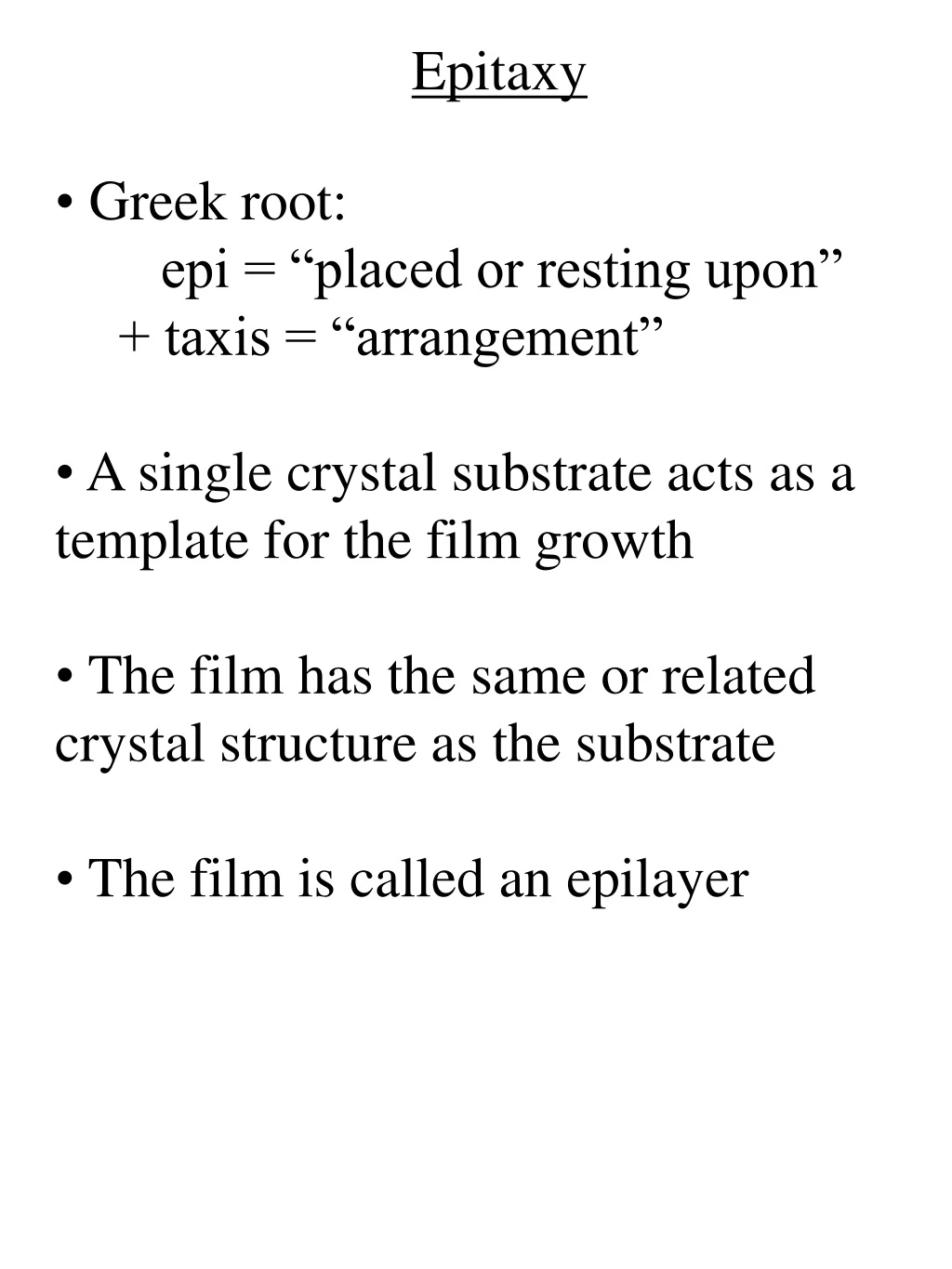
Epitaxy • Greek root: • epi = “placed or resting upon” • + taxis = “arrangement” • A single crystal substrate acts as a template for the film growth • The film has the same or related crystal structure as the substrate • The film is called an epilayer
Semiconductor Substrates • Single crystal wafer sliced from boules using diamond saws • 400 – 500 mm thick • Chemical and mechanical polishing produces a smooth surface From Grovenor, Fig. 2.10, p. 72
Substrates • (100)±1° oriented substrates most common • Flats indicate wafer alignment and doping type • p-type: Be, Zn • n-type: Sn, Si • semi-insulating (SI): Fe(deep acceptor) From Sze, Fig. 12, p. 315
Substrates • Substrate Preparation • Thermal outgassing • Oxide desorption (thermal, sputtering, ECR plasma, atomic hydrogen)
Epitaxy Epitaxy Homoepitaxy Heteroepitaxy Film and substrate are different materials (e.g., InGaAsP on InP, SiGe on Si) Film and substrate are the same material (e.g., Si on Si, InP on InP)
Epitaxy • Why homoepitaxy ? • The film can be made more free of defects, purer than the substrate and can be doped independently of the substrate • Why heteroepitaxy ? • Ability to control bandgap • Heterostructures can be created to confine electrons and light (e.g., quantum wells)
Lattice-Matching af From Ohring, Fig. 7-1, p. 308 as Misfit, f = (as – af) / af f = 0 for lattice-matched (LM’d) films f > 0 for tensile strain f < 0 for compressive strain f < 5 x 10⁻⁴ considered “good” (LM’d)
Heteroepitaxy • Cubic crystals develop tetragonal distortion (strain) to achieve the same in-plane lattice constant as the substrate (Da/a)┴ = [(1+n)/(1-n)] (Da /a)o n = Poisson’s ratio af as From Ohring, Fig. 7-1, p. 308
Heteroepitaxy • Define the strain, • ef = (af|| - af)/af Initially the film grows with ef = f af as From Ohring, Fig. 7-1, p. 308
Heteroepitaxy • The film will relax beyond a certain “critical thickness” or “critical misfit” • Then 0 < ef < f af as From Ohring, Fig. 7-1, p. 308
Misfit Dislocations From Mayer, Fig. 6.19, p. 164
Misfit Dislocations From Mayer, Fig. 14.17, p. 426
Misfit Dislocations From Grovenor, Fig. 3.20, p. 146
Lattice-Matching Ohring Fig. 7-15, p. 328
Lattice-Matching • In1-xGaxAs1-yPy From Panish & Temkin, Fig. 1.5, p. 9
Energetics • What is the “critical thickness” or “critical misfit” ? • Elastic strain energy per unit area: • Es = [ 2m (1 + n) / (1 – n) ] ef2d • ef = film strain = (af|| - af)/af • = f initially • m = film shear moduli • n = Poisson’s ratio • d = film thickness
Energetics • Dislocation energy per unit area: • Ed = [ mb (f – ef) / (2p (1-n)) ] • ln (Ro/b + 1) • d = film thickness • n = Poisson’s ratio • b = dislocation Burgers vector • Ro = radius about the dislocation • where strain field terminates
Misfit Dislocations From Mayer, Fig. 6.20, p. 164
Energetics • Dislocations are energetically more favorable than strain beyond a certain critical thickness or misfit From Grovenor, Fig. 3.18, p. 141
Critical Strain • Minimize the total energy with respect to strain: • d(Es + Ed)/def = 0 • Solving gives the critical strain beyond which dislocations are favorable: • ef* = [ b / ( 8p(1+n)d) ] ln (Ro/b + 1) d = film thickness n = Poisson’s ratio b = dislocation Burgers vector Ro = radius about the dislocation where strain field terminates
Critical Thickness • Assume ef* = f for d < d* • Assume fully relaxed layer beyond the critical thickness, i.e., ef* = 0 for d > d* • Assume Ro ~ d* • Critical thickness, • d* = [ b / ( 8p(1+n)f) ] ln (d*/b + 1)
Energetics • Dislocations are energetically more favorable than strain beyond a certain critical thickness or misfit From Mayer, Fig. 14.16, p. 425
Critical Thickness From Grovenor, Table 3.4 & 3.5, p. 143
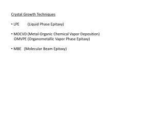
Epitaxial Techniques Epitaxy VPE MBE MO Sources Solid Sources Hydride Sources SSMBE HSMBE MOMBE
Molecular Beam Epitaxy • Separate sources for group III, group V and dopant atoms From Ohring, Fig. 7-21, p. 338
Molecular Beam Epitaxy • UHV conditions required for sample purity • Cryopanels (hollow wall filled with liquid nitrogen) used to prevent water vapor & volatile contaminants from impinging on sample; cryopanels act as a fast pump • Mean free path of atoms or molecules in the beams > source-substrate distance • Molecular flow = source atoms experience no collisions during their travel time
MBE History • Developed by A. Y. Cho, J. R. Arthur at Bell labs • Late 60’s to early 70’s • First MBE-grown material was GaAs • Motivation was GaAs/AlGaAs & InGaAsP lasers for telecommunications
Why MBE ? • Ability to produce thin layers (quantum wells) • Ability to produce abrupt interfaces • Ability to produce abrupt compositional changes (heterostructures) • Ability to produce abrupt doping profiles (concentration and type of dopant)
Solid Sources • Effusion cells (PVD) • Group III (In, Ga, Al) • Group V: Sb, As • Dopants • n-type: Si, Sn • p-type: Be, Zn • semi-insulating (SI): Fe From Ohring, Fig. 7-21, p. 338
Solid Sources From Herman et al, Fig. 6.3, p. 87
Solid Sources • Flux controlled by temperature and shutters • Recall Langmuir relation: z = P / ( 2pmkT)½ • P = Po exp(DSvap/k) exp (-DHvap / kT)
Solid Sources • To achieve |f | < 10-3 in InGaAs, need • Dx < 1% • DTIn, Ga < ± 0.5 °C • Solid sources determine uniformity of growth (thickness and composition) • Substrate rotation required
Substrate Holder • Provides sample rotation (magnetic coupling) • Provides a heater to achieve desired substrate temperature; temperature uniformity is important for composition uniformity across the sample • Sample is held mechanically (clips) or with In solder
Substrate Temperature Measurement • Thermocouple • Beneath sample holder • Calibrated to a phase transition (e.g., melting point of In) • Calibration can change during growth of small bandgap epilayers due to radiative heating • Accuracy is ± 10 °C for thermocouple behind sample • ± 2 °C for thermocouple in contact with sample From Panish & Temkin, Fig. 4.6, p. 89
Substrate Temperature Measurement • Pyrometer • Periscope arrangement prevents coating of window during deposition • Bandgap changes during heterostructure growth can affect the reflectivity • Reflections from opening and closing of shutters, coating of viewport, and changes in sample emissivity may confuse the temperature • Calibration required From Panish & Temkin, Fig. 4.8, p. 91
Shutters Allow rapid switching (~0.1 s) of beam flux From Panish & Temkin, Fig. 4.4, p. 83
Phosphorous • Problems with Solid P & As Sources • Large exponential dependence of vapor pressure on temperature of solid As and P • Large VP of As and P demands large effusion cells; difficult to control temperature uniformly • P contains allotropes with different VP; leads to control problems and thermal history • P4, As4 are produced from solid sources which have low sticking probabilities; requires V/III ratio for tetramers ~50; requires large pumping speeds
Hydride Sources (HSMBE, GSMBE) • Cracking cell uses high temperatures (1000 °C) and a catalyst (Ta or Rh) to decompose AsH3 and PH3 into dimers: • 2AsH3 → As2 + 3H2 • 2PH3 → P2 + 3H2 • Large amounts of H2 produced; requires good pumping From Ohring, Fig. 7-21, p. 338
Hydride Sources From Panish & Temkin, Fig. 3.15 & 3.16, p. 72
Hydride Sources • Equilibrium curves indicate that dimers are the dominant species at 1000 °C (typical Ptotal ~ 10-3 Torr) From Panish & Temkin, Fig. 3.8 & 3.9, p. 67
MOMBE • MOMBE uses metalorganic compound sources • Group III sources are metalorganic (MO) • Group V sources are MO or hydrides From Panish & Temkin, Fig. 4.27, p. 117
MOMBE • Advantages compared to MBE: • Fewer hot sources (no group III effusion cells) • Infinite source supply • Single (mixed) group III beam for improved compositional uniformity • Advantages compared to MOVPE: • No boundary layer problems for scale-up • Beam nature for abrupt interfaces • UHV permits in situ characterization
MOMBE • Group III sources are metalorganic (MO) From Panish & Temkin, Fig. 2.20, p. 41
MOMBE • Group III metalorganics (MO) are cracked on the growth surface From Panish & Temkin, p. 42
MOMBE • Group V sources: • Pre-cracked MO or hydrides • DEA = (CH3CH2)2AsH • MEA = (CH3CH2)AsH2 • TBA = (CH3)3AsH2 From Panish & Temkin, Fig. 2.30, p. 53
MOMBE • Dopants • Solid: Be, Sn • Hydrides: SiH4, Si2H6, GeH4 cracked on substrate • MO: TESn, DEBe, DEZn cracked on substrate From Panish & Temkin, Fig. 5.2, p. 122
Gas Handling • Pressure-regulated control (PRC) From Panish & Temkin, Fig. 4.13, p. 97
Gas Handling • Pressure-regulated control (PRC) From Panish & Temkin, Fig. 4.14, p. 98
Gas Handling • Mass flow control (MFC) From Panish & Temkin, Fig. 4.15, p. 99 From Herman et al, Fig. 8.16, p. 181
Gas Handling • Mass flow control (MFC) From Panish & Temkin, Fig. 4.16, p. 100