Download
1 / 16
160 likes | 277 Views
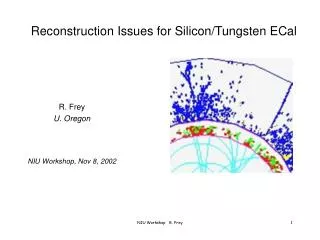
Silicon-Tungsten EM calorimeter. Rémi Cornat Laboratoire Leprince-Ringuet Ecole Polytechnique – IN2P3/CNRS On behalf of the SiW -ECAL ILD project * w ithin CALICE coll. From this. t o this :. H CAL. ECAL. A mix of technologies validated with prototypes.

E N D
Silicon-Tungsten EM calorimeter Rémi Cornat Laboratoire Leprince-Ringuet Ecole Polytechnique – IN2P3/CNRS On behalf of the SiW-ECAL ILD project* within CALICE coll.
From this... to this: HCAL ECAL A mix of technologies validated with prototypes
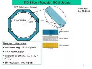
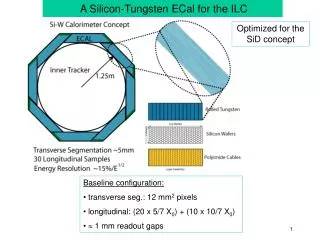
First prototype (2006) : validation of physics perf. First generation prototype and tested on beam 2006-2008 30 layers - ~10000 channels Mechanical structure: carbon fibre composite, incorporating tungsten layers Standard printed circuit slabs hold silicon sensors & electronics (outside detection area) S/N ~ 7.5
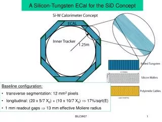
Calorimeters for ILC ECAL : ~24 X0, 20 cm thick ~2500 m2 active detectors ~100M readout channels Reduce dead material, calorimeters inside coil, Extreme compactness Work with specific beam structure ILC: 5Hz trains each of 3k bunches @ 340 ns low occupancy, low noise : S/N >10
Technological prototype (2011) : Proof of feasibility → embedded “system on chip” electronics, → extremely low power consumption typ. 25 µW/ch, → wide sensors (81 cm², pure silicon), → large composite mechanical structure, → readout technology insensitive to ~4T field, → integrated DAQ system Goal : 1 instrumented tower (40k channels, 20 cm2 crossection)
Large mechanical structure done Each layer build separately then “coked” together. Deeply simulated : mechanical constraints, thermal behavior Next step : wider assembly with 5 columns Tungsten plates wrappedintocarbon fibre: 15 layers 7 mm tick detector slabslidedintoalveola
Detector slab : “extreme” design Compact assembly of 2 layers of 1 to 8 Active SensorUnits (ASU) 1 ASU = 1 kapton (HV bias for PIN diodes) + 1 layer PIN diodes + 1 PCB withmicrochipsembeded + 1 thermal drain (copper) PCB iscritical : 1 mm tick, 8 layers, 1% flatness , chips boundedinto Short version Heat shield PCB wafer glue Kapton film
PIN diode matrices design The simplest design to control the cost • Few thousands of m² needed for ILD • Glued on PCB : Floating Guard Rings Drawbacks : • Large dead zone at the edges (>1 mm) • Crosstalk with GR R&D in close collaboration with HPK • Split GR and/or complete removal of GR • Laser dicing : gain a factor 2 on dead zone • Smaller size abutted matrices may improve yield Also tried edgeless techno. from VTT P++ implants (pixels) Guard Rings I region N++ implant HPK : 9x9 cm², 256 pixels
SKIROC chip SiliconKalorimeterIntegrated Read Out Chip • TechnologySiGe 0.35µm AMS. • Production batch received Q3’10 • 64 channels, variable gain charge amp, 12-bit ADC, digital logic • Power-pulsed → 25 μW/channel Power pulsing • Variable currentconsumption according to state • 1 slab : 0 to 10 Amps pulses of 1 ms at 5 Hz
Detector slab : conservative design Same concepts but with chips in package • BGA design requires additional 3 mm in SLAB thickness • Ultra thin BGA under study : promising • Feasibility of lidframe : done • Impact on Xtalk, noise : to be studied • Length of pixel-chip traces divided by 2-3 w.r.t. PQFP design Advanced package technologies • Thicknesses as low as 0.5mm • Ball bonded Flip chip • Allow efficient routing of pcb traces and digital/analog separation : longest analog trace is ~2 cm (today prototype are build using PQFP to ease debugging) BGA pattern : 1/16th of the PCB
Long SLAB assembly Up to 9 equipped PCBs interconnected to make detector slab Electrical and mechanical connection made thanks to Kapton connecting cable Technique under investigation • Soldering with Flat Cable (Kapton) • Easy for mass production Full size kapton for interconnects 18 cm, 4 slots of 36 pins each
Developing a leakless water cooling system Total ECAL power dissipation O(10 kW) even at 25 µW/ch Need active cooling system (cold water pipe + radiator) Limit : temperature differences within ECAL heat transfer to neighboring detectors Thermal simulations of detector modules Cooling tests in demonstrator module
DAQ : hardware and software • Scalable : Computing network architecture • Standard : Giga-Ethernet, Serial 8b10B • Backplane-less • Compact • “one cable for everything” • Data Acquisition, Timing, Slow control • Flexible and highlymodularsoftware • Multiple output formats • Files (offline) • Shared memory (online H. Perf) • TCPSockets (remote online) • Subsampling(real time processing) • Used for test beams
Assembly of first SLABs Most of technologies described above used to build first SLABs First approach of an assembly procedure Toward automation and indistrialization Simplified SLABS including 1 ASU with 4 SKIROCs in PQF package 1 Si Wafer (256 chn) Succesfuly put into structure
First 6 SLABS tested @DESY (July’12) Seenext talk S/N > 14
Summary CALICE Si-W ECAL technologies with emphasis on • Low power FE electronics incorporated in detector volume • Integration (Structure, DAQ, cooling, services) • Sensor improvements & industrialization Step by step prototyping allow tracking the best feasibility/cost compromise Optimization of overall design is based on accurate physics simulations • Number of layers • Number of pixels • Dead area • Allowed material Connection between 2 A.S.U. • Now have a good understanding of how to build a complete ECAL • with affordable technologies