Download
1 / 13
130 likes | 202 Views
Learn about innovative analog-to-digital converter technology for 60 GHz radios, focusing on energy efficiency using deep sub-micron CMOS technologies.

E N D
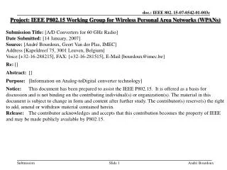
Project: IEEE P802.15 Working Group for Wireless Personal Area Networks (WPANs) Submission Title: [A/D Converters for 60 GHz Radio] Date Submitted: [14 January, 2007] Source: [André Bourdoux, Geert Van der Plas, IMEC] Address [Kapeldreef 75, 3001 Leuven, Belgium] Voice:[+32-16-288215], FAX: [+32-16-281515], E-Mail:[bourdoux@imec.be] Re: [] Abstract: [] Purpose: [Information on Analog-toDigital converter technology] Notice: This document has been prepared to assist the IEEE P802.15. It is offered as a basis for discussion and is not binding on the contributing individual(s) or organization(s). The material in this document is subject to change in form and content after further study. The contributor(s) reserve(s) the right to add, amend or withdraw material contained herein. Release: The contributor acknowledges and accepts that this contribution becomes the property of IEEE and may be made publicly available by P802.15. André Bourdoux
A/D converters for 60GHz radio André Bourdoux Geert Van der Plas André Bourdoux
A/D research: innovative A/D solution for 60GHz radios Radio Receiver Energy-efficient, reconfigurableanalog-to-digital converters in deep sub-micron CMOS technologies for 60GHz wireless systems ADC Digital FE Analog FE André Bourdoux
The ADC FoM, the energy per conversion step EQ, is the energy efficiency measure • P is the power consumption • empirically EQhas been found to be almost constant for a given technology independent of fsampleor effective number of bits (ENOB), hence a FoM. • A value of 1 pJ/step is/was considered good • current best public known value is 0.16pJ/step • This FoM is also our measure for reconfigurable A/D: halving speed should halve power, removing one bit also André Bourdoux
Deep sub-micron CMOS enables better energy efficiency • FoM is dependent on technology • example: CMOS scaling has enabled reduction from 8.2 pJ/step (0.25u) to 0.16 pJ/step (90nm) for GS/s 4-6b flash converters • Target technology is 65/45nm • invent new or modify existing architectures to exploit the potential energy efficiency enabled by scaling André Bourdoux
60 GHz radios require 4-6 bit, GS/s A/D:Energy Efficiency is at best 0.16 pJ/step André Bourdoux
SNDR versus fin, fs=1.25 GS/s ENOB @ nyquist = 3.7 ERBW = 3.3 GHz SNDR [dB] André Bourdoux
Spectrum @ nyquist, fs=1.25 GS/s SFDR = 36 dB 2500pts André Bourdoux
Zoom-in on waveform @ 3.6 GHz, fs=1.25 GS/s André Bourdoux
100 mW 10 mW 1 mW In 65/45 nm CMOS, A/D consume ~10 mW if we can maintain energy efficiency @ 0.1pJ • Assume a 0.1 pJ/step energy efficiency • a 4b, 4GS/s A/D ~6.4 mW • a 5b, 2GS/s A/D ~6.4 mW • a 6b, 2GS/s A/D ~12.8 mW • etc. André Bourdoux
A/D technology can reach the 0.1pJ target in 65nm two power suppliesbuffer & core(both 1.8V for 0.18u) single-endedtime multiplexedoutputs (2) serial inputdata & clock Chip: 4b 1GS/s0.8pJ in 0.18u, 4b1.25GS/s 0.16pJ in 90nm single-endedclock input differential input André Bourdoux
Designs in the pipeline • two 90nm designs are planned for early next year (tape out Q1 2007) • 5b ~2GS/s target power 10mW (0.15 pJ/step) • 6b ~1GS/s target power 10mW (0.15 pJ/step) • 65nm designs (tape out Q3 2007) • increase sampling speed and improve energy efficiency (0.1pJ/step) André Bourdoux
References • Van der Plas, G.; Decoutere, S.; Donnay, S., “A 0.16pJ/Conversion-Step 2.5mW 1.25GS/s 4b ADC in a 90nm Digital CMOS Process”, ISSCC 2006 André Bourdoux