Download
1 / 14
310 likes | 785 Views
Wire-bonding interconnections. Our experiences at the ASIC-Lab Heidelberg. Overview. Introduction Technology (Ball vs. Wedge) Industry Limits or Standards? Bondtests (3) Design for Bonding (2) (Un)Related Obstacle (3). Introduction.

E N D
Wire-bonding interconnections Our experiences at the ASIC-Lab Heidelberg Workshop on Silicon Detectors Systems for the CBM experiment
Overview • Introduction • Technology (Ball vs. Wedge) • Industry Limits or Standards? • Bondtests (3) • Design for Bonding (2) • (Un)Related Obstacle (3) Workshop on Silicon Detectors Systems for the CBM experiment
Introduction A Wire Bonding Definition:It’s a solid phase metal welding process using heat, pressure and/or ultrasonic Power to bond a wire to a pad by means of electron sharing or interdiffusion of atoms. • Al Bond Wires are alloyed with 1%Si or 1%Mg • Au Bond Wires are doped with 10ppm Be or 100ppm Cu • Also insulated Bond Wires are available } Pure Al or Au is to soft Workshop on Silicon Detectors Systems for the CBM experiment
Ball vs. Wedge Workshop on Silicon Detectors Systems for the CBM experiment
Industry Limits wedge 45µmball 60µm (2005) • Minimum Bond pitch: 35µm (15µm Wire) • > 3000 interconnections • Process Stability: 40ppm failure rate Industry Standards? • A Bond pitch of 100µm is welcome • 350 Interconnections are still a lot • Process Stability: 2% failure rate (Yield of 98% warranty) Workshop on Silicon Detectors Systems for the CBM experiment
Bondtests (1/3) Pull strength vs. Wire deformation By increasing power, time, force and (possibly) heat, the bond foot will stick better to the pad but in the same time the wire will be flattened and the bond heel will become weaker. foot tail heel High reproducibility is a key factor so the optimum bonding parameters are found within the breakage region, directly after, but less than the maximum bond strength. This achieves maximum reproducibility and high bond strength. Workshop on Silicon Detectors Systems for the CBM experiment
Bondtests (2/3) Destructive bond pull test The Destructive bond pull test, is the primary method to evaluate the bond strength by hooking and pulling the bonded wire until failure occurs. The purpose of this test is to examine the bond strength and to certify the proper setup of the bonding parameters. The results are important for evaluating bonding quality and reliability, as well as understanding bond failure mechanisms like cratering, Pull force dependents on the geometrical configuration of the pulling test. For absolute values, the pull test has to be be normalized. The force in each wire with the pull force at hook (F) is represented by this parallelogram of forces. In practise one should take care, that both angles are nearly the same. => F1 = F2 = F / 2 sin The failure during pull test may occur at one of the five positions: A. Lift off first bond B. Wire break at the heel of the first bond C. Wire break mid Loop D. Wire break at the heel of the second bond E. Lift off second bond When properly pulled and bonded, the bond should fail at B or D. Workshop on Silicon Detectors Systems for the CBM experiment
Bondtests (3/3) Bondability- Process Capability index To assure the stability of the bond process you have to verify the bondability of you devices. Typically this will be checked as a incoming components inspection on a sample of each MCM Substrates lot. The forces of the bond pull test can be expected to be normal distributed. With the mean value and the sigma one can calculate the Process Capability index (Cpk). (mean value – lower limit) Cpk= (3 * standard deviation) a Cpk of at least 1.33 is desired ~ failure rate 40ppm The lower limit may vary!MIL-STD-883E:2.5cN for 25µm Al wire Assembly company: 7cN for 30µm Al wire (without normalisation) Cpk=0.66 Cpk=1.00 Cpk=1.33 Cpk=1.66 This Cpk definition is for processes with only a lower limit! Workshop on Silicon Detectors Systems for the CBM experiment
Design for Bonding (1/2) 25µm Al double stackered wedge bonding Chipcore Chipedge DieSeal IO Structure Workshop on Silicon Detectors Systems for the CBM experiment
Design for Bonding (2/2) Life is not easy - Boards have to be cost effective and signal tracks have to assure signal quality in first place .. but then, talk to the guy who has to do the bonding. Life is not easy Life is not easy - Boards have to be cost effective and signal tracks have to assure signal quality in first place • “45 degrees” is the max fan-out angle • With wires of the same length, the bonds get the same loop form (easier) • The pattern recognition likes position markers Workshop on Silicon Detectors Systems for the CBM experiment
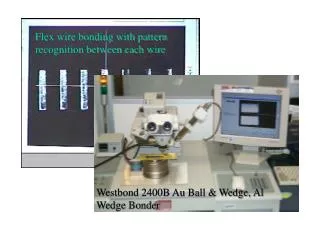
(Un)Related Obstacle (1/3) Flexprint Flex materials like polyamide absorb some of the Ultrasonic Power If the flexprint is a multilayer design, then different optimum Bond parameters can occur on each pad. Workshop on Silicon Detectors Systems for the CBM experiment
(Un)Related Obstacle (2/3) Surface Pores Scratches Contamination Workshop on Silicon Detectors Systems for the CBM experiment
(Un)Related Obstacle (3/3) Glob top • Glob top is the industry standard for sealing chips on board, this Epoxy Grout comes in many viscosities, and colours. The temperature coefficient of thermal expansion fits printed circuit boards made of FR4 quite well. • But larger Glob top get problems, separate chips if possible. • Glob tops absorb moisture, glob toped boards which should be soldered have to be baked out first. Workshop on Silicon Detectors Systems for the CBM experiment
References • The Nordic Electronics Packaging Guideline on Wire Bonding: http://extra.ivf.se/ngl/documents/ChapterA/chapterA.pdf • A German Script about the processing of dice(FH München, Labor für Aufbau und Verbindungstechnik)http://www.lme.fh-muenchen.de/avt_2005_Diemontage.pdf(Page 12-44) Workshop on Silicon Detectors Systems for the CBM experiment